Gate charge and switching loss budget
Total gate charge is 31 nC at 10 V, with 1240 pF input capacitance at 100 V drain bias. At a 100 kHz hard-switching frequency, the gate drive must supply roughly 3.1 mA average current — a standard 1 A driver handles it with margin. The 57 W package-level power dissipation limit means the thermal path through the PowerFlat™ exposed pad is the real constraint in a 650 V flyback or PFC stage.
Package and thermal interface
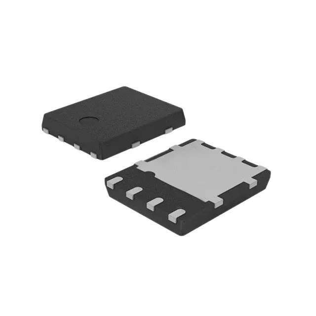
Housed in the 8-lead PowerFlat™ 5x6 mm surface-mount package with an exposed drain pad. The copper area on the PCB under the pad sets the junction-to-ambient thermal resistance — a 25 mm² pad on a 2 oz copper board typically keeps the junction below 125°C at 15 A continuous in still air. The 150°C maximum junction temperature leaves headroom for transient overloads.
