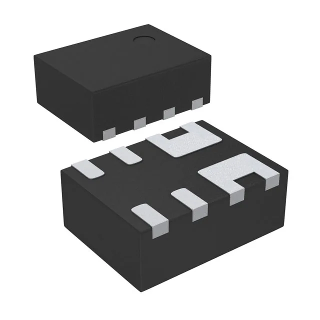
Package and board-fit — the 8-FC-TDFN (1.5x2)
The SLG59M1496V comes in an 8-FC-TDFN (1.5x2) package — a 1.5 mm x 2 mm footprint with an exposed pad underneath. The package's low profile and small land pattern mean the solder-paste stencil aperture for the exposed pad needs to be around 50-60% coverage to avoid voiding — a solid stencil will trap flux and cause tombstoning on the small signal pads.
What the 7.8 mOhm Rds(on) means at 5.3 A
With a typical on-resistance of 7.8 mOhm, the conduction loss at 5.3 A is about 0.22 W (I²R). The switch is a high-side N-Channel with a 1:1 input-to-output ratio, meaning it passes the full supply voltage to the load with no boost converter.
Lifecycle and compliance — active and RoHS
No stock-holding claim; availability verified per quote.
How it compares to the SLG59M301V
The closest functional peer is the SLG59M301V, also a high-side N-Channel load switch in the same GreenFET family. The SLG59M1496V offers lower Rds(on) (7.8 mOhm vs 8.5 mOhm) and higher continuous current (5.3 A vs 4.0 A). Both share the same 1:1 ratio, CMOS input, and -40°C to 85°C temperature range. The SLG59M301V uses the same 8-FC-TDFN (1.5x2) package and pinout — it is a drop-in replacement for BOMs where the load current is under 4 A and the slightly higher Rds(on) is acceptable. For a 5 A rail, the SLG59M1496V is the correct fit.