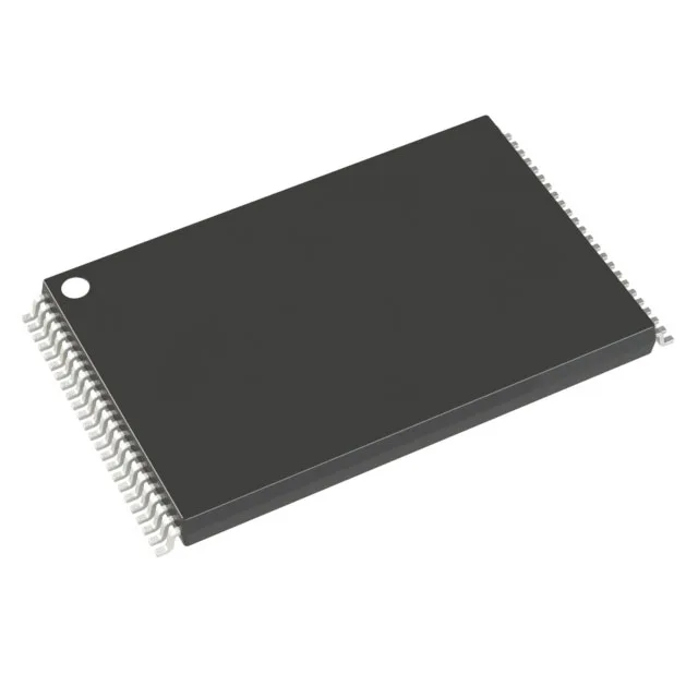
The Renesas RMLV1616AGSA-5S2#AA0 is a 16Mbit parallel SRAM organized as 2M x 8 or 1M x 16, with a 55 ns access time. That 55 ns window covers address-to-data-valid on reads and write-cycle completion — it sets the minimum bus cycle period for a memory transaction. For a 3.3 V system running a 20 MHz bus clock (50 ns period), this part leaves essentially zero margin for address decode and board trace delay; you will need to insert wait states or stretch the bus cycle. At 10 MHz (100 ns period) it fits cleanly with about 45 ns of timing slack.
The 55 ns write-cycle time (word and page modes) matches the read access, so back-to-back read/write sequences do not introduce an asymmetry penalty.
Housed in a 48-TFSOP (0.724", 18.40 mm width) surface-mount package, also designated as 48-TSOP I. The body is 18.4 mm wide with a 0.5 mm pin pitch typical of TSOP-I. The Tray shipping medium is standard for this package — no tape-and-reel suffix, so plan for hand-placement or a tray feeder if using automated pick-and-place. The footprint is shared across several Renesas 16Mbit SRAMs in the same package, easing a second-source qualification if needed.