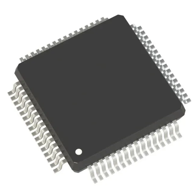
Renesas Electronics R7F100GPJ3CFA#AA0 — Microcontrollers & Processors (MCU / MPU / DSP)

R7F100GPJ3CFA#AA0 Renesas RL78/G23 16-bit MCU, 32 MHz

MPNR7F100GPJ3CFA#AA0
End of Life

Renesas RL78/G23 16-bit MCU, R7F100GPJ3CFA#AA0, 32 MHz, 256 KB Flash, 24 KB RAM, 8 KB EEPROM, 88 I/O, 100-LQFP, -40 to 105 °C.

$4.48Ref. price · indicative, final on quote
Packaging100-LQFP
RoHSROHS3 Compliant
SeriesRL78/G23
Sourced new & surplus through independent channelsAuthenticity-screened · ESD-safe packingListing updated Aug 2026

Specifications

R7F100GPJ3CFA#AA0 specifications
ParameterValue
SeriesRL78/G23
MountingSurface Mount
Oscillator typeInternal
Program memory typeFLASH
Voltage - supply (Vcc (Vdd))1.8V ~ 5.5V
Operating temperature-40°C ~ 105°C (TA)
Speed32MHz
PackageTray
RAM size24K x 8
Core size16-Bit
EEPROM size8K x 8
PeripheralsCapacitive Touch, LVD, POR, PWM, WDT
ConnectivityCSI, I²C, LINbus, SPI, UART/USART
Number of i (O)88
Core processorRL78
Case100-LQFP
Data convertersA/D 20x10b, 8x12b; D/A 2x8b
Program memory size256KB (256K x 8)

Product details

RL78/G23 16-bit MCU with 32 MHz core and 256 KB Flash

An additional 8 KB of EEPROM data flash provides non-volatile parameter storage without external parts. The device integrates a 20-channel 10-bit ADC, an 8-channel 12-bit ADC, and a 2-channel 8-bit DAC, covering most analog front-end needs for sensor conditioning and closed-loop control. The 88 I/O lines in a 100-LQFP package (14x20 mm) offer ample pin budget for parallel displays, keypads, and multi-axis actuator interfaces.

There is no announced end-of-life, no last-time-buy window, and no successor mandate. For a procurement desk qualifying a BOM line, that means no supply disruption from an imminent phase-out.

Memory headroom and analog integration

The 256 KB Flash is sized for moderate firmware with a bootloader and OTA staging area; the 24 KB RAM handles real-time data buffers for multi-channel ADC acquisition and communication stacks. The 8 KB EEPROM block supports wear-leveled parameter storage — useful for calibration coefficients or fault logs that survive power cycles without external serial EEPROM. The dual ADC resolution (10-bit and 12-bit) lets the designer trade conversion speed for precision: the 12-bit channels suit temperature or pressure sensing, while the 10-bit channels handle faster current or voltage monitoring loops.

Because the part is active and not in a constrained allocation phase, lead times typically track the manufacturer's standard factory cycle. For dual-sourcing or second-source qualification, the RL78/G23 family includes pin-compatible siblings with the same 88 I/O count and 100-LQFP footprint — the key difference is Flash and RAM density, not function.

Frequently asked questions

Where can I buy R7F100GPJ3CFA#AA0?

Pricing and stock are confirmed at the time of quote — submit an inquiry for a current price and delivery estimate.

Does R7F100GPJ3CFA#AA0 have a direct second-source or equivalent?

The RL78/G23 family includes several pin-compatible siblings in the same 100-LQFP package with 88 I/O. The R7F100GPG3CFB#AA0 is one such variant; it shares the same core, speed, peripheral set, and temperature range, but with different Flash/RAM densities. No identical second-source from another manufacturer exists — Renesas is the sole source for this architecture.

What is the programming interface for R7F100GPJ3CFA#AA0?

The RL78/G23 uses Renesas's single-wire or two-wire debug interface (emulator or emulator) for programming and debugging. BOOT0 pin strapping selects the boot source; the debug port remains active even with the watchdog enabled.

Is R7F100GPJ3CFA#AA0 compatible with 3.3 V logic?

At 3.3 V operation, all I/O pins are 5 V tolerant, so direct connection to 5 V peripherals is possible without level shifters on most pins.