Active production — no end-of-life concern for new designs
The R5F5651EHGLJ#20: ROHS3 compliance means no exemption-based supply chain risk — the part ships without lead, mercury, or restricted phthalates under the current EU directive.
120 MHz RXv2 core with 2 MB flash — real-time control headroom
The RXv2 core runs at 120 MHz — this is the throughput ceiling for nested interrupt service routines and control loops. The 32 KB EEPROM stores calibration coefficients and fault logs, eliminating a separate serial EEPROM from the BOM. The 29-channel 12-bit ADC samples multiple analog inputs — current sensors, thermistors, potentiometers — in a single conversion sequence. The dual 12-bit DAC generates analog setpoints or reference voltages for external regulators or amplifiers. Both converters share the internal oscillator, so no external crystal is required for the conversion clock.
Ethernet, CAN, USB — industrial gateway and drive connectivity
The peripheral set includes Ethernet, CANbus, USB, and QSPI — the three interfaces that dominate industrial communication. Ethernet handles Modbus TCP or EtherNet/IP; CANbus covers CANopen or J1939 on the drive network; USB provides a local programming or data-logging port. The QSPI interface connects to external NOR flash or SRAM for data buffering. The 111 I/O pins leave room for parallel LCD buses, external memory interfaces, and sensor arrays. The EBI/EMI interface allows direct connection to external SRAM, SDRAM, or FPGA dual-port memory without a glue-logic CPLD. For motor-drive applications, the PWM timer channels generate complementary dead-time-controlled outputs for three-phase inverter stages.
100-TFLGA 7x7 mm — board integration checklist
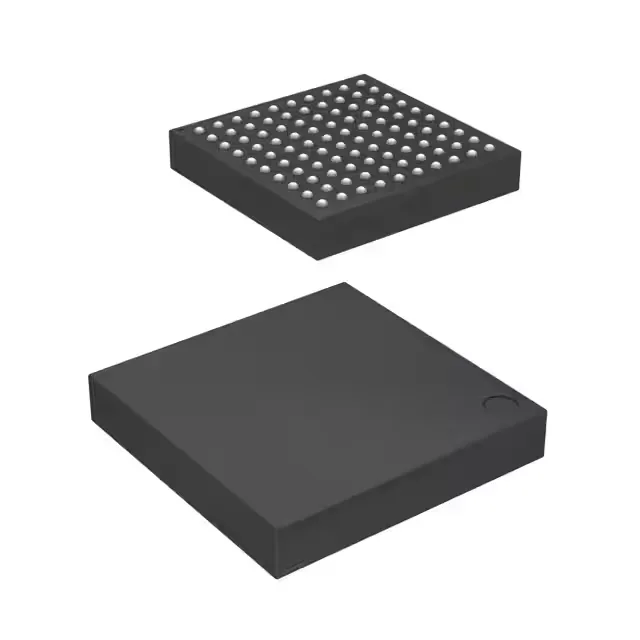
The 100-TFLGA package measures 7x7 mm with a 0.50 mm ball pitch. This is a land-grid array, not a BGA — the pads are flat lands, not solder balls, so the reflow profile follows the JEDEC LGA standard. The surface-mount footprint requires a solder-paste stencil thickness of 0.125 mm for consistent joint height.