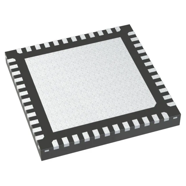
Renesas Electronics R5F51406ADNE#30 — Microcontrollers & Processors (MCU / MPU / DSP)

R5F51406ADNE#30 Renesas RX140 32-bit MCU, 48 MHz

MPNR5F51406ADNE#30
End of Life

Renesas RX140 series 32-bit MCU, RXv2 core, 48 MHz, 256 KB Flash, 64 KB RAM, 8 KB EEPROM, CANbus/I²C/SCI/SPI, 39 I/O, 11-ch 12-bit ADC, -40 to 85°C, 1.8-5.5 V, 48-WFQFN exposed pad.

$3.64Ref. price · indicative, final on quote
Packaging48-WFQFN Exposed Pad
RoHSROHS3 Compliant
SeriesRX140
Sourced new & surplus through independent channelsAuthenticity-screened · ESD-safe packingListing updated Aug 2026

Specifications

R5F51406ADNE#30 specifications
ParameterValue
SeriesRX140
MountingSurface Mount
Oscillator typeInternal
Program memory typeFLASH
Voltage - supply (Vcc (Vdd))1.8V ~ 5.5V
Operating temperature-40°C ~ 85°C (TA)
Speed48MHz
PackageTray
RAM size64K x 8
Core size32-Bit Single-Core
EEPROM size8K x 8
PeripheralsCapacitive Touch, DMA, LVD, POR, PWM, Temp Sensor, WDT
ConnectivityCANbus, I²C, SCI, SPI
Number of i (O)39
Core processorRXv2
Case48-WFQFN Exposed Pad
Data convertersA/D 11x12b
Program memory size256KB (256K x 8)

Product details

48 MHz RXv2 core with 256 KB Flash — what the memory and speed buy you

The Renesas R5F51406ADNE#30 is a 32-bit single-core MCU from the RX140 series, built around the RXv2 CPU core running at 48 MHz. The 48 MHz clock, combined with the DMA controller, handles sensor fusion loops and communication protocol stacks (CAN, I²C, SCI, SPI) without stalling the core on each byte transfer.

Industrial temperature range and wide supply — where it goes on the board

The 39 available I/O include capacitive touch channels, PWM outputs, and a 12-bit ADC with 11 multiplexed inputs — enough for a control panel with a touch interface, a few analog sensors, and a CAN bus to the host controller.

Active lifecycle — no end-of-life clock ticking

R5F51406ADNE#30 carries an active product status. The ROHS3 compliance is confirmed.

Frequently asked questions

Can R5F51406ADNE#30 be used with existing RX140 code?

Yes. The R5F51406ADNE#30 is part of the RX140 series with the same RXv2 core at 48 MHz. Firmware written for other RX140 variants is binary-compatible at the instruction-set level, though peripheral and pin-mapping differences (39 I/O vs 53 I/O on the R5F51406AGFM#30) require a review of the BSP and pin configuration files.

What is the closest functional equivalent to R5F51406ADNE#30?

The R5F51406AGFM#30 is the same RX140 series, same 48 MHz RXv2 core, same 256 KB Flash, and same peripheral set (CAN, I²C, SCI, SPI, capacitive touch, DMA, PWM). The package differs — R5F51406AGFM#30 comes in a Tray, not the 48-WFQFN. If you need more I/O or a wider temperature grade, that is the pin-compatible step-up.