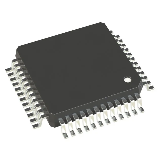
RXv2 core at 48 MHz — memory map and peripheral fit
The R5F51405BGFL#30 is a 32-bit single-core MCU built around the RXv2 core, clocked at 48 MHz. This is the entry point of the RX140 series — the core delivers a single-cycle multiply and a hardware divider, so the 48 MHz ceiling is not a bottleneck for control-loop or sensor-fusion tasks that stay within the flash wait-state profile. On-chip memory: 128 KB of program flash, 32 KB of SRAM, and a separate 8 KB data flash that doubles as EEPROM emulation. The 8 KB data flash is organized for byte-rewrite — a firmware parameter table or calibration constant can be updated in-field without wearing the main flash array. The wide Vcc envelope also tolerates a discharged battery or a long PCB trace drop — the internal LDO and POR handle the brownout edge.
Peripheral set — what the 39 I/O lines bring
On-chip peripherals include a 12-bit ADC with 11 channels, a capacitive touch sensing unit, a temperature sensor, a true random number generator (TRNG), and an AES accelerator. The TRNG and AES block together enable on-the-fly encryption of firmware updates or sensor data without a separate crypto coprocessor. Connectivity: CAN bus (one channel), I²C, SCI (UART/synchronous), and SPI. The SCI modules support asynchronous and clock-synchronous modes — a single SCI line can drive a debug UART and a SPI sensor by reconfiguring the pin function at runtime.
Temperature grade and operating envelope
An enclosure that sees 85°C internal air on a hot day still leaves 20°C of junction headroom before the silicon derating curve starts to limit the clock frequency.