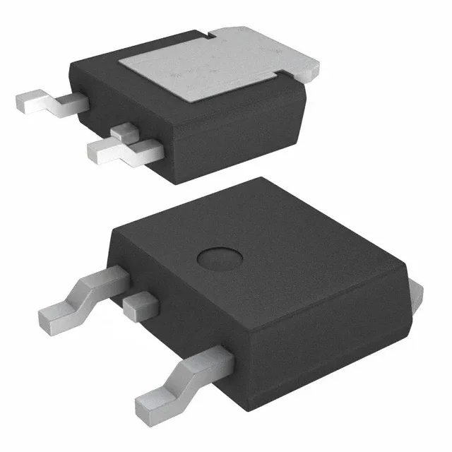
The NP60N055VUK-E1-AY: With Rds(on) specified at 5.5 mOhm max at Vgs = 10 V and Id = 30 A, the conduction loss at full rated current is under 20 W at 25 °C junction — but the 1.2 W ambient power dissipation limit means the PCB copper area and airflow must handle the thermal load. The 63 nC total gate charge at 10 V is moderate: a typical gate-driver IC sourcing 1 A peak can switch this MOSFET in under 100 ns, keeping crossover losses manageable at switching frequencies up to 100 kHz.
Active lifecycle — BOM-fit for production
The TO-252-3 package is widely second-sourced; the reel and cut-tape options suit both prototyping and volume assembly.
Package and thermal — TO-252-3 layout notes
The 105 W case-limited power dissipation assumes the tab is connected to a sufficient thermal plane; without it, the 1.2 W ambient limit applies.