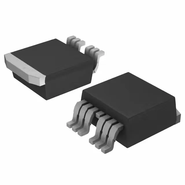
The NP180N055TUK-E1-AY: The TO-263-7 (D²Pak with 6 leads plus tab) surface-mount package dissipates 348 W at case temperature and 1.8 W in still air at ambient.
Gate charge and switching — what 294 nC means for the driver
Total gate charge is 294 nC at 10 V. That is a heavy gate — at 50 kHz switching, the average gate-drive current works out to about 14.7 mA, but the peak current the driver must source to charge the gate in the desired transition time is what determines the driver's peak output capability. Plan for a driver rated at least 2 A peak to keep the switching edge under 100 ns. That large Ciss, combined with the gate charge, means the driver sees a capacitive load that slows the turn-on edge if the drive current is limited. The Miller plateau region will be pronounced; a gate resistor in the 5–10 Ohm range helps control ringing without stretching the switching loss window too far.
The NP180N055TUK--AY carries an active product status. The operating junction temperature range extends to 175 °C, which suits high-side switching in under-hood automotive modules or industrial power supplies.
How it compares to the NP179N055TUK-E1-AY
The NP179N055TUK--AY is the closest functional sibling: same 55 V Vdss, same 180 A Id rating, same TO-263-7 package, and same 4 V threshold at 250 µA. The differences are in the on-resistance and gate charge — the NP180N055TUK--AY offers 1.4 mOhm Rds(on) versus 1.75 mOhm, and 294 nC Qg versus 240 nC. The lower Rds(on) reduces conduction loss by about 20 % at full current, but the higher gate charge demands more from the driver. The NP179N055TUK--AY also carries AEC-Q101 automotive qualification, which the NP180N055TUK--AY does not explicitly list.