55 V, 110 A — the power-switch tier this part fills
The NP110N055PUK-E1-AY: N-Channel MOSFET, 55 V drain-source, 110 A continuous drain. Requires 10 V gate drive for minimum on-resistance.
Thermal reality: 348 W at case, 1.8 W at ambient
The power dissipation spec tells the real story: 348 W maximum when the case temperature is held at 25 °C, but only 1.8 W when the ambient air is 25 °C. The operating junction temperature is rated to 175 °C, which is typical for automotive-grade power MOSFETs and gives some headroom in a thermally marginal layout.
TO-263 (D²Pak) — surface-mount power footprint
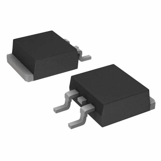
The NP110N055PUK--AY comes in a TO-263-3 package, also called D²Pak (2 leads plus tab). The tab is the drain terminal — the PCB land pattern needs a large copper area with thermal vias to inner layers to pull heat away from the junction.
Peer comparison: NP179N055TUK-E1-AY
It shares the same 55 V drain-source rating, same 1.75 mOhm Rds(on) at 10 V, and same 175 °C junction temperature, but it is rated for 180 A continuous drain — 70 A more than the NP110N055PUK--AY. Its gate charge is lower at 240 nC, which reduces driver losses at high frequency. The NP179N055TUK--AY also carries AEC-Q101 automotive qualification, making it the preferred choice for under-hood or chassis-domain applications where the NP110N055PUK--AY lacks that certification.