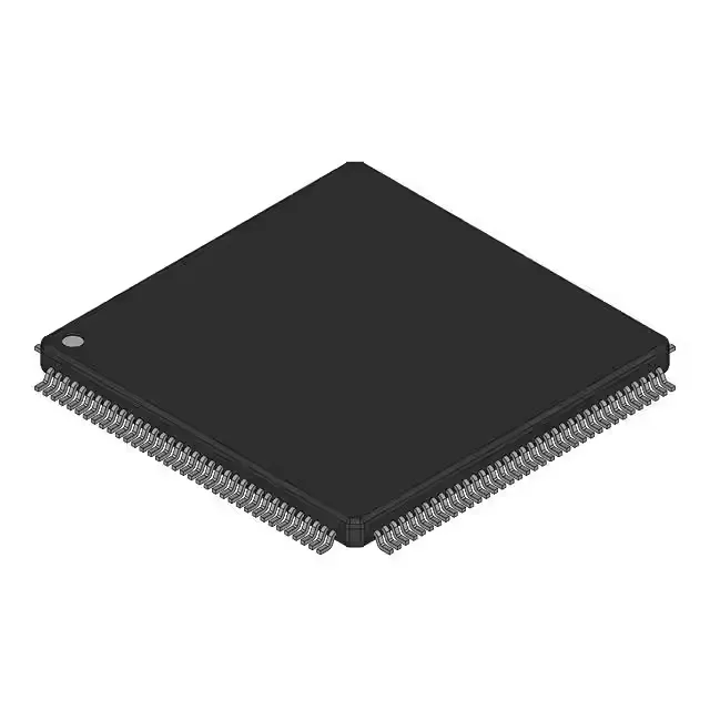
Package and board-fit — 144-LQFP integration demands
The M32171F2VFP ships in a 144-LQFP package (supplier device package 144-LFQFP, 20x20 mm).
Memory budget and core throughput
384 KB of on-chip FLASH program memory (384K x 8) and 16K x 8 SRAM provide the code and data space for a real-time control stack plus a moderate-size application buffer. The 40 MHz M32R core delivers roughly 40 MIPS, assuming one instruction per clock for most ALU operations — sufficient for CAN message handling and PID-loop closure at sub-millisecond rates. At 5 V the core draws higher dynamic current at 40 MHz; the thermal budget in the 144-LQFP should account for the worst-case power dissipation at the upper temperature corner.
Peripheral set — CAN, ADC, and PWM for control nodes
CANbus connectivity (with EBI/EMI, SPI, and UART/USART) makes this MCU a natural fit for distributed control nodes in automotive body electronics or industrial automation backplanes. The 16-channel 10-bit ADC and single 10-bit DAC handle sensor acquisition and analog output without external converters in cost-sensitive designs. DMA and PWM peripherals offload the CPU for data transfers and waveform generation. With 97 I/O lines, the part can interface to parallel LCDs, external SRAM via the EBI, or a bank of discrete sensors without a port expander.
Renesas lists the M32171F2VFP as Active (current production).