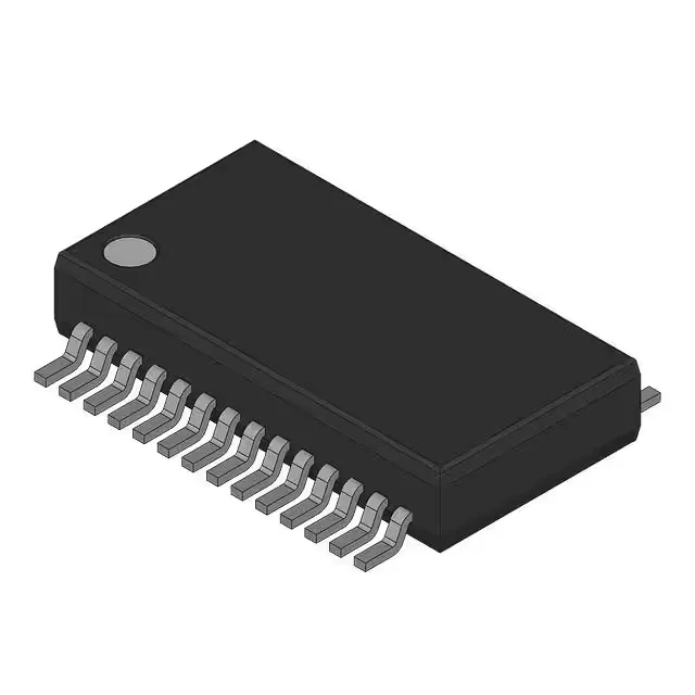
Renesas Electronics IDT74FCT162823BTPV — Microcontrollers & Processors (MCU / MPU / DSP)

IDT74FCT162823BTPV Renesas 18-bit D-Type Register, 15ns

MPNIDT74FCT162823BTPV
End of Life

Renesas Electronics IDT74FCT162823BTPV, FAST 18-Bit Register, D-Type, Positive Edge Triggered, Tri-State Non-Inverted Outputs, 56-TFSOP (4.40mm Width), Surface Mount, Bulk.

$1.31Ref. price · indicative, final on quote
Packaging56-TFSOP (0.173", 4.40mm Width)
StockIn Stock (25)
Lead timeIn Stock wk
MOQ1 pcs
  • 100% new & originalTraceable channels only — no refurbs, no pulls, no remarked parts.
  • Date & lot codes on quoteStated per line before you commit; label photos on request.
  • MSL-compliant ESD packingMoisture-sealed bags with indicator cards; reels photo-verified.
  • PayPal buyer protectionPay by T/T, PayPal or Payoneer — card payments covered end to end.

Specifications

IDT74FCT162823BTPV Technical Specifications
ParameterValue
TypeD-Type
Output typeTri-State, Non-Inverted
Trigger typePositive Edge
Mounting typeSurface Mount
Voltage4.5V ~ 5.5V
Current - quiescent500 µA
Current - output high, low24mA, 24mA
Operating temperature-40°C ~ 85°C (TA)
PackageBulk
FunctionStandard
Case56-TFSOP (0.173\", 4.40mm Width)
Input capacitance3.5 pF
Number of elements2
Number of bits per element9
Max propagation delay @ v, max CL15ns @ 5V, 300pF

Product details

18-bit bus-interface register in TVSOP-56

The Renesas IDT74FCT162823BTPV is an 18-bit D-type register built on the FAST FCT logic family. It packages two 9-bit elements in a single 56-pin TVSOP body (4.40 mm width) for surface-mount assembly. Each element captures data on the positive edge of the clock and drives the bus through tri-state, non-inverted outputs. The 24 mA symmetric output drive handles moderate capacitive loads on short backplane or memory-interface traces.

Timing and supply margins for the BOM

Maximum propagation delay is 15 ns into a 300 pF load at 5 V supply. This sets the data-to-output settling window for the receiving latch — budget the 15 ns plus clock-to-output skew when calculating the bus cycle time. Quiescent current is 500 µA typical; the dynamic draw scales with the output toggle rate and load capacitance. Input capacitance is 3.5 pF per pin — a light load on the upstream driver.

Production status and compliance flag

RoHS compliance is not claimed for this variant — the part is listed as RoHS non-compliant. Verify the board-level assembly requirements before specifying this order code for a lead-free reflow profile.

Frequently asked questions

What is the propagation delay of IDT74FCT162823BTPV?

Maximum propagation delay is 15 ns into a 300 pF load at 5 V supply. This is the spec for the data-to-output path from clock edge.

What package does IDT74FCT162823BTPV use?

56-TFSOP (0.173", 4.40 mm width) with a surface-mount footprint. The supplier device package is 56-TVSOP.