PLL with bypass — the clock-tree decision point
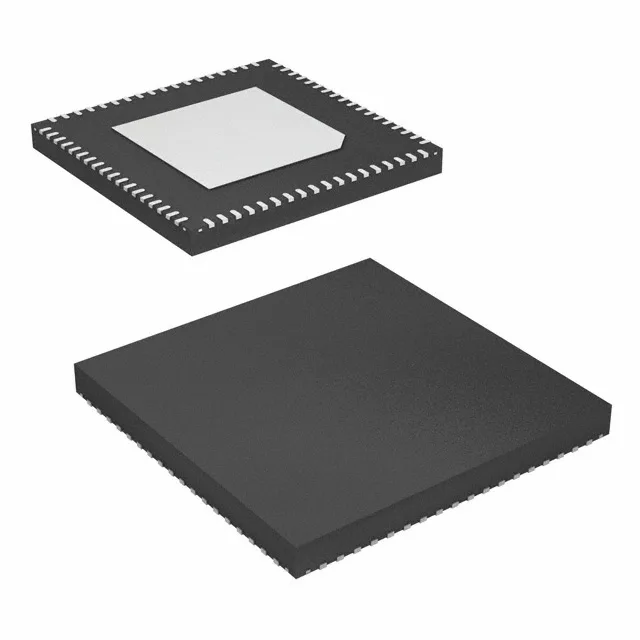
The 9ZML1252EKILF is a PLL-based clock generator with a bypass path — when the PLL is engaged it cleans up jitter on the input reference, and in bypass mode the input passes through to the outputs with minimal added phase noise. This dual-mode capability means a single part can serve both a clean, synthesised clock tree and a low-latency fanout path on the same board. It accepts two HCSL inputs and distributes them to twelve HCSL outputs, all differential — the 2:12 ratio gives enough fanout for a PCIe reference clock tree feeding multiple endpoints from one device. The maximum output frequency hits 400 MHz, which covers PCIe Gen 1 through Gen 4 reference clock rates and most SerDes PLL reference requirements.
Supply rail and temperature — the operating envelope
The supply voltage is 3.135 V to 3.465 V — a tight 3.3 V nominal range. The PLL's jitter performance is sensitive to supply noise; a clean 3.3 V rail with less than 50 mV ripple is expected for the datasheet jitter numbers to hold.
Active lifecycle — no LTB clock ticking
The single-circuit design means one PLL core per package — no shared resources between channels, so each output pair sees independent jitter from the others.
No stock-holding claim; the part is procured per order.