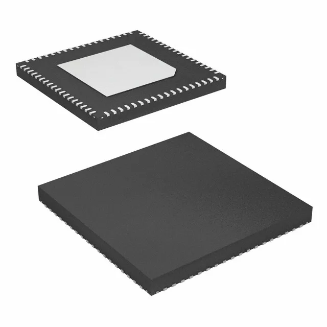
PLL clock buffer with 2:12 HCSL fanout
The Renesas 9ZML1233EKILF is a PLL clock buffer with bypass capability, designed to distribute a single HCSL input to twelve HCSL outputs at frequencies up to 400 MHz. The 2:12 input-to-output ratio means one reference clock feeds a dozen destinations, which is useful for fanning out a common timing reference across multiple PCIe or Ethernet interfaces on the same board. Both input and output are differential HCSL, so the signal integrity budget stays tight across the fanout tree — no single-ended conversion losses between the reference and the loads.
Package and rework considerations
Surface-mount only, supplied in tray format — no tape-and-reel, so pick-and-place feeders need tray handling or a tube adapter.
Supply voltage and bypass mode
Runs from a single 3.3V supply (3.135V to 3.465V), which is the standard rail for HCSL clock distribution — no additional voltage regulator needed if the board already has a 3.3V plane. The PLL bypass mode lets the input clock pass through to the outputs without jitter cleaning, which is useful when the reference is clean enough and you only need fanout, not frequency synthesis. No internal divider or multiplier (Divider/Multiplier: No/No), so the output frequency equals the input frequency — this is a pure fanout buffer, not a frequency synthesizer.