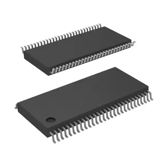
PLL clock generator for Intel CPU and PCIe clock trees
The 9LPRS525AGLFT is a PLL-based clock generator IC designed to produce the reference clocks for Intel CPU platforms and PCI Express lanes. It takes a single crystal input and fans it out to 19 differential clock outputs, covering the full clock tree for a desktop or server motherboard without needing multiple oscillators. The 1:19 input-to-output ratio means one device replaces what would otherwise be a discrete PLL plus a separate fanout buffer — the PLL cleans up the crystal jitter, and the fanout delivers matched-length differential pairs to each PCIe slot and chipset block.
400 MHz differential outputs and supply rail tolerance
Maximum output frequency is 400 MHz, which covers the 100 MHz PCIe reference clock (Gen1-3) plus any CPU base clock stretching up to 400 MHz for overclocking or turbo modes. The outputs are differential — the No/Yes entry under Differential - Input:Output means the crystal input is single-ended, but all 19 clock outputs are differential pairs (typically HCSL or similar), which is what PCIe receivers expect. The PLL's internal VCO and charge pump are regulated from this rail, so a clean 3.3 V supply with under 50 mV ripple is assumed for rated jitter performance. This part is intended for controlled-environment equipment — desktop PCs, servers in data centres, or test equipment with forced air.
56-TSSOP package and board integration
Routing 19 differential pairs out of this package on a 4-layer board is feasible but requires careful impedance control — the 400 MHz edges have sub-ns rise times that will couple into adjacent traces if the ground plane is not continuous under the fanout region.
Active lifecycle and compliance status
ROHS3 compliant — the part contains no restricted substances above the threshold limits, and it is lead-free per the EU RoHS directive. No additional exemptions or transition periods apply.