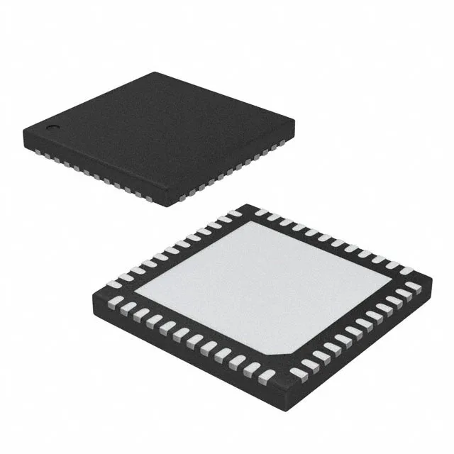
Renesas Electronics 9FGV0841AKLF — Clock & Timing ICs

9FGV0841AKLF PCIe Clock Generator, 100 MHz, 48-VFQFPN

MPN9FGV0841AKLF
End of Life

Renesas 9FGV0841AKLF PCI Express (PCIe) clock generator, PLL-based, 100 MHz max frequency, HCSL and LVCMOS outputs, 1:9 input-to-output ratio, 1.7V-1.9V supply, 48-VFQFPN (6x6 mm) package, 0°C to 70°C operating temperature.

$4.07Ref. price · indicative, final on quote
Packaging48-VFQFN Exposed Pad
StockContact for availability
MOQ1 pcs
  • 100% new & originalTraceable channels only — no refurbs, no pulls, no remarked parts.
  • Date & lot codes on quoteStated per line before you commit; label photos on request.
  • MSL-compliant ESD packingMoisture-sealed bags with indicator cards; reels photo-verified.
  • PayPal buyer protectionPay by T/T, PayPal or Payoneer — card payments covered end to end.

Specifications

9FGV0841AKLF Technical Specifications
ParameterValue
Mounting typeSurface Mount
Voltage1.7V ~ 1.9V
Frequency100MHz
Operating temperature0°C ~ 70°C
PLLYes
InputCrystal
OutputHCSL, LVCMOS
PackageTray
Main purposePCI Express (PCIe)
Case48-VFQFN Exposed Pad
Number of circuits1
Ratio - Input:Output1:9
Differential - Input:OutputNo/Yes

Product details

PCIe clock generator — what the 9FGV0841AKLF does on your board

The Renesas 9FGV0841AKLF is a PLL-based clock generator purpose-built for PCI Express (PCIe) reference clock distribution. It takes a single-ended crystal input and produces up to nine differential HCSL or single-ended LVCMOS output copies at frequencies up to 100 MHz. The 1:9 input-to-output ratio means one clean reference fans out to nine PCIe lanes or endpoints — exactly what a multi-slot backplane or a switch-fabric card needs. The commercial temperature range (0°C to 70°C) suits controlled indoor equipment — server motherboards, network switches, storage arrays, and testers. For extended-temperature or outdoor deployment, look at the -40°C to 85°C rated 9ZXL0851EKKLF or 9ZXL1231EKILF instead.

Output type and PCIe generation support

The differential input-to-output flag reads No/Yes — meaning the crystal input is single-ended, but all nine clock outputs are differential (HCSL). That conversion is exactly what a PCIe clock tree needs: clean differential distribution from a low-cost crystal source.

Frequently asked questions

What is the output type of 9FGV0841AKLF?

The 9FGV0841AKLF outputs HCSL (differential) and LVCMOS (single-ended) levels. The HCSL outputs are the primary PCIe reference clock signals; LVCMOS can drive legacy logic or sideband clocks on the same die.

Is 9FGV0841AKLF available in tape and reel packaging?

The base order code 9FGV0841AKLF ships in a Tray. The tape-and-reel variant uses the suffix 'T' — 9FGV0841AKLFT — and is electrically identical. Confirm the reel suffix before ordering for pick-and-place feeders.

Can 9FGV0841AKLF be used for PCIe Gen4 clocking?

The part is rated to 100 MHz maximum, which is the standard PCIe reference clock frequency for Gen1 through Gen3. Gen4 at 16 GT/s typically requires tighter phase-jitter specifications; verify against your root-complex or switch device's jitter tolerance mask before committing the BOM for a Gen4-only design.

What is 9FGV0841AKLF's listed PLL status?

The PLL field is Yes — this is a PLL-based clock generator, not a simple buffer or fanout. The internal PLL synthesizes the output clocks from the crystal input.

What is 9FGV0841AKLF's listed input type?

The input is a Crystal. The part accepts a fundamental-mode crystal as its reference, not a single-ended clock or differential oscillator. This keeps the BOM cost low by using a passive crystal rather than an active oscillator module.