Renesas Electronics 9DML0441AKILFT — Clock & Timing ICs

9DML0441AKILFT PCIe Clock Buffer, 200 MHz, 2:4 HCSL

MPN9DML0441AKILFT
End of Life

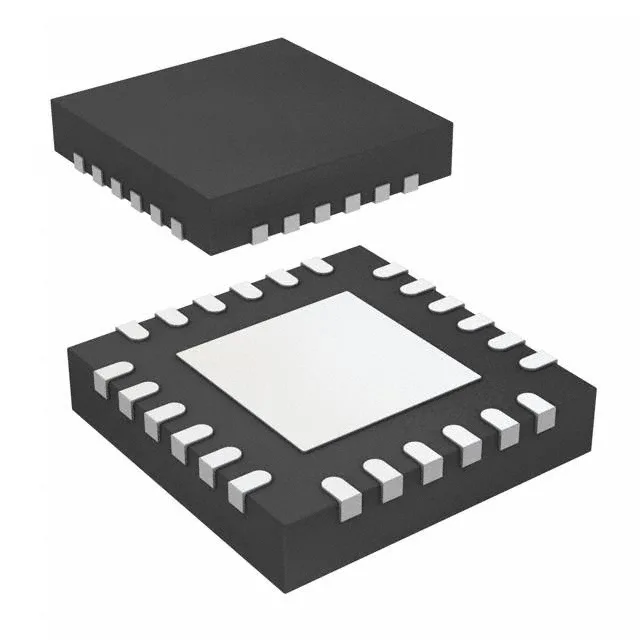
Renesas 9DML0441AKILFT, PCI Express (PCIe) clock buffer, 2:4 HCSL fanout, no PLL, 200 MHz max, 3.135V–3.465V supply, -40°C to 85°C, 24-VFQFPN (4x4) package.

$4.34Ref. price · indicative, final on quote
Packaging24-VFQFN Exposed Pad
StockContact for availability
MOQ1 pcs
  • 100% new & originalTraceable channels only — no refurbs, no pulls, no remarked parts.
  • Date & lot codes on quoteStated per line before you commit; label photos on request.
  • MSL-compliant ESD packingMoisture-sealed bags with indicator cards; reels photo-verified.
  • PayPal buyer protectionPay by T/T, PayPal or Payoneer — card payments covered end to end.

Specifications

9DML0441AKILFT Technical Specifications
ParameterValue
Mounting typeSurface Mount
Voltage3.135V ~ 3.465V
Frequency200MHz
Operating temperature-40°C ~ 85°C
PLLNo
InputHCSL
OutputHCSL
PackageTape & Reel (TR); Cut Tape (CT)
Main purposePCI Express (PCIe)
Case24-VFQFN Exposed Pad
Number of circuits1
Ratio - Input:Output2:4
Differential - Input:OutputYes/Yes

Product details

PCIe reference clock distribution without the PLL

The Renesas 9DML0441AKILFT is a 2:4 fanout buffer for PCI Express reference clocks, accepting two differential HCSL inputs and delivering four HCSL outputs at up to 200 MHz. It contains no PLL — the outputs are a clean, low-jitter copy of the input, with no frequency multiplication or spread-spectrum synthesis. That makes it a fit for PCIe Gen1 and Gen2 root-complex-to-slot clock trees where the reference already meets the jitter spec and you just need to split the signal without adding phase noise.

200 MHz ceiling and the PCIe generation it serves

Rated for a maximum output frequency of 200 MHz, this buffer covers the 100 MHz reference clock used by PCIe Gen1 and Gen2, plus any 125 MHz or 200 MHz non-PCIe differential clocks in the system. It does not support the 400 MHz references that Gen3 and Gen4 PLL-based buffers handle — if your design targets Gen3 or later, you need a part with a PLL, such as the 9DB803DFLFT (1:8, 400 MHz, PLL-based).

Industrial temperature range — wider than the typical PCIe buffer

Rated for -40°C to 85°C operating temperature, this part suits outdoor telecom cabinets, industrial backplanes, and engine-bay-adjacent electronics where the ambient can swing well beyond the 0°C to 70°C range of many PCIe clock buffers. The 9DBL411BGLFT, for example, is limited to 0°C to 70°C, so if your BOM calls for a wider temperature grade, the 9DML0441AKILFT is the drop-in candidate.

Package and supply — standard PCIe footprint

Housed in a 24-VFQFPN with exposed pad (4x4 mm), the part is surface-mount and requires the pad to be soldered to a ground plane for thermal and electrical integrity. Supply voltage is 3.3 V ±5% (3.135 V to 3.465 V), the standard PCIe clock buffer rail. The exposed pad must be connected to ground — a via array under the pad is recommended for heat spreading.

Lifecycle and sourcing

The 9DML0441AKILFT carries an Active lifecycle status with ROHS3 compliance. It is not nearing end-of-life, so it can be specified into new designs without an LTB risk.

Frequently asked questions

What is the difference between the 9DML0441AKILFT and the 9DML0441BKILFT?

The evidence does not contain specifications for the 9DML0441BKILFT variant, so a direct comparison cannot be made. The 9DML0441AKILFT is a 2:4 HCSL fanout buffer with no PLL, 200 MHz max, and -40°C to 85°C range.

What is the closest functional second-source for the 9DML0441AKILFT?

The 9DBL411BGLFT is a similar PCIe clock buffer with a 1:4 fanout ratio and LP-HCSL outputs, but it has a lower 150 MHz max frequency and a 0°C to 70°C temperature range. It is not a direct pin-compatible replacement — verify the fanout ratio and temperature grade against your BOM.