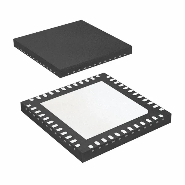
Active production — BOM-fit for PCIe and Ethernet clock trees
The 9DBV0841AKILF: Its primary purpose is clock distribution for Ethernet and PCI Express interfaces, making it a direct fit for server, switch, and line-card boards that need low-jitter reference clocks at up to 137.5 MHz.
The device operates from a 1.7 V to 1.9 V supply, a narrow range typical of 1.8 V-core clocking ICs — the board's 1.8 V rail must stay within ±5.6 % to keep the PLL locked and the output swing within HCSL specs. Both input and output are differential HCSL, so the signal integrity budget is set by the trace impedance and termination, not the single-ended noise margin — common in PCIe Gen1/2/3 reference clock designs.
Surface-mount assembly with a tray shipping medium means the parts are loose in matrix trays, not tape-and-reel — factor this into the pick-and-place feeder setup if the line expects reeled components.
Fully ROHS3 compliant, with no exemption conflicts for EU or UKCA markets — the part carries no lead, mercury, or restricted phthalates above the threshold.