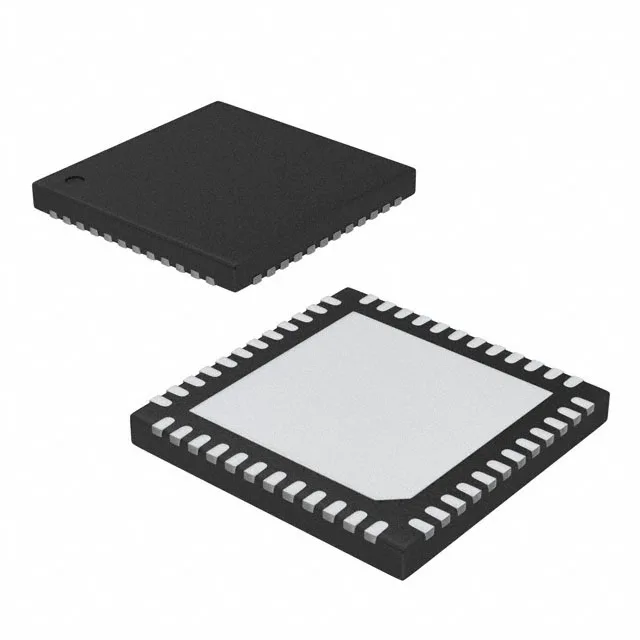
Renesas Electronics 9DBU0841AKLF — DC-DC Power Modules

9DBU0841AKLF PCIe Clock Buffer, 1:8 Fanout, 167 MHz

MPN9DBU0841AKLF
End of Life

Renesas 9DBU0841AKLF PCI Express (PCIe) clock buffer, PLL Yes, 1:8 fanout, HCSL input to LP-HCSL output, 167 MHz max, 1.5 V supply, 48-VFQFN Exposed Pad, 0°C to 70°C.

$4.84Ref. price · indicative, final on quote
Packaging48-VFQFN Exposed Pad
StockContact for availability
MOQ1 pcs
  • 100% new & originalTraceable channels only — no refurbs, no pulls, no remarked parts.
  • Date & lot codes on quoteStated per line before you commit; label photos on request.
  • MSL-compliant ESD packingMoisture-sealed bags with indicator cards; reels photo-verified.
  • PayPal buyer protectionPay by T/T, PayPal or Payoneer — card payments covered end to end.

Specifications

9DBU0841AKLF Technical Specifications
ParameterValue
Mounting typeSurface Mount
Voltage1.425V ~ 1.575V
Frequency167MHz
Operating temperature0°C ~ 70°C
PLLYes
InputHCSL
OutputLP-HCSL
PackageTray
Main purposePCI Express (PCIe)
Case48-VFQFN Exposed Pad
Number of circuits1
Ratio - Input:Output1:8
Differential - Input:OutputYes/Yes

Product details

PCIe clock distribution — what this buffer does on the board

The Renesas 9DBU0841AKLF is a 1:8 PCI Express clock buffer with an integrated PLL, fanning out a single HCSL reference clock to eight LP-HCSL outputs. It runs on a 1.425V to 1.575V supply rail.

1:8 fanout — enough for a multi-slot backplane

One input drives eight output copies. That's enough to clock a half-dozen PCIe slots plus the chipset on a standard ATX server board, or to distribute the refclk across a compact PCIe switch fabric. The differential input and output (Yes/Yes) keep signal integrity intact across the fanout tree — no single-ended conversion losses to budget for.

Temperature grade — indoor equipment only

Rated 0°C to 70°C, so this part belongs in a temperature-controlled server room, telecom central office, or office equipment — not in an outdoor base station or under-hood automotive ECU. If your BOM calls for a wider range, the 9ZXL0851EKKLF covers -40°C to 85°C but runs on a 3.135 V supply and uses standard HCSL outputs, not LP-HCSL.

Package and footprint — 48-VFQFPN, 6x6 mm

The 6x6 mm exposed pad needs a thermal via pattern under the pad for the supply rail's return current. The exposed pad is the ground connection — don't leave it floating. Surface-mount only; no through-hole equivalent exists.

Sourcing and lifecycle — active, no LTB risk

The 9DBU0841AKLF is listed as Active and ROHS3 compliant. For dual-sourcing, the closest functional peer is the 9DB803DFLFT — same 1:8 fanout, same PCIe purpose, but its output is standard HCSL (not LP-HCSL) and it runs on a 3.135 V supply, so the rail and output swing differ. A direct drop-in it is not; verify the downstream receiver's input threshold before swapping.

Frequently asked questions

Can the 9DBU0841AKLF be used in PCIe Gen3 applications?

Yes. The 167 MHz maximum frequency covers the 100 MHz reference clock rate used by PCIe Gen1, Gen2, and Gen3. The PLL and LP-HCSL outputs meet the jitter and swing requirements for Gen3 refclk distribution.