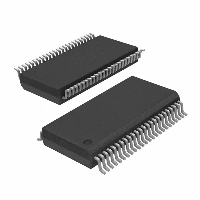
Renesas Electronics 9DB803DFILF — Discrete Semiconductors

Renesas 9DB803DFILF PCIe Clock Buffer, 400MHz, 1:8, 48-SSOP

MPN9DB803DFILF
End of Life

Renesas Electronics PCI Express (PCIe) clock buffer, PLL Yes, 1:8 fanout, 400 MHz max, HCSL input/output, 48-BSSOP (0.295", 7.50mm Width), Surface Mount, Tube.

$5.75Ref. price · indicative, final on quote
Packaging48-BSSOP (0.295", 7.50mm Width)
StockIn Stock (23)
Lead timeIn Stock wk
MOQ1 pcs
  • 100% new & originalTraceable channels only — no refurbs, no pulls, no remarked parts.
  • Date & lot codes on quoteStated per line before you commit; label photos on request.
  • MSL-compliant ESD packingMoisture-sealed bags with indicator cards; reels photo-verified.
  • PayPal buyer protectionPay by T/T, PayPal or Payoneer — card payments covered end to end.

Specifications

9DB803DFILF Technical Specifications
ParameterValue
Mounting typeSurface Mount
Voltage3.135V ~ 3.465V
Frequency400MHz
Operating temperature-40°C ~ 85°C
PLLYes
InputHCSL
OutputHCSL
PackageTube
Main purposePCI Express (PCIe)
Case48-BSSOP (0.295\", 7.50mm Width)
Number of circuits1
Ratio - Input:Output1:8
Differential - Input:OutputYes/Yes

Product details

PCIe clock distribution in a 48-SSOP footprint

The 9DB803DFILF is a 1:8 differential fanout buffer with an integrated PLL, designed to distribute a clean 400 MHz reference clock across a PCI Express (PCIe) clock tree. The 48-SSOP package (7.50 mm body width) demands a standard surface-mount footprint — no fine-pitch rework required, though the 0.295-inch lead span means the board layout should match the SSOP land pattern, not a narrower SOIC. Input and output are both HCSL (High-Speed Current Steering Logic), the de facto signaling standard for PCIe reference clocks. The differential I/O path (Yes/Yes) means the buffer preserves signal integrity across the fanout — each of the eight outputs drives a separate HCSL-compliant load without the skew accumulation you'd see from a daisy-chain.

Supply headroom and temperature grade

If your board's 3.3 V rail droops below 3.135 V under load, the PLL may lose lock; budget the IR drop across the PCB trace and the regulator's load regulation into that floor. The industrial temperature grade (-40°C to 85°C) covers most outdoor and factory-floor deployments — an engine bay or direct-sunlight enclosure at 85°C ambient still leaves margin before the junction limit. At 400 MHz max frequency, this buffer supports PCIe Gen 1 through Gen 3 reference clock rates (100 MHz, 125 MHz, and the spread-spectrum variants). The 1:8 fanout ratio means a single input drives up to eight loads — useful for distributing the reference to multiple root complexes, switches, or endpoint PHYs without an external clock divider.

Frequently asked questions

What is the closest functional second-source for the 9DB803DFILF?

The 9DB803DFILF is the industrial-temperature (-40°C to 85°C) tube-packaged variant. For a drop-in replacement without rewiring, verify your board's temperature requirements — the 9DB803DFLFT will not meet the full industrial range.

What is the 9DB803DFILF's PLL and input/output type?

The 9DB803DFILF integrates a PLL (Yes) and uses HCSL signaling for both input and output. The differential I/O path (Yes/Yes) supports PCIe reference clock distribution at up to 400 MHz with a 1:8 fanout ratio.