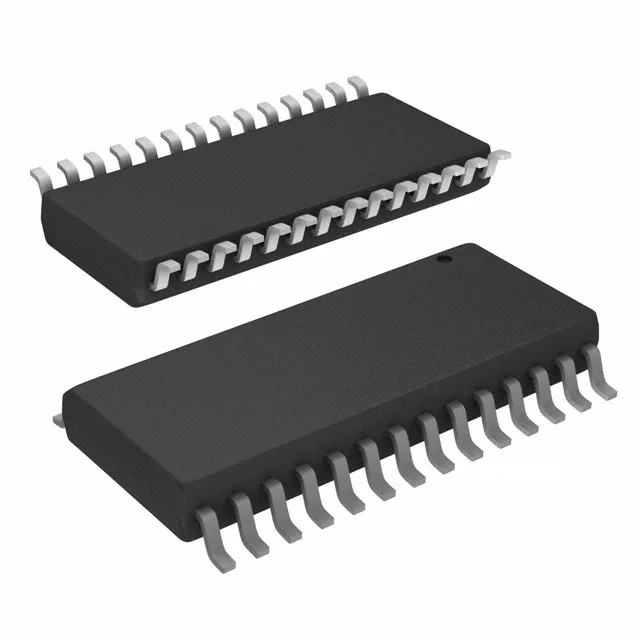
Renesas Electronics 9DB403DFLFT — Discrete Semiconductors

Renesas 9DB403DFLFT PCIe Buffer, 1:4 HCSL/LVDS, 400 MHz

MPN9DB403DFLFT
End of Life

Renesas Electronics 9DB403DFLFT PCI Express (PCIe) clock buffer, PLL Yes, 1:4 fanout, HCSL input, HCSL/LVDS output, 400 MHz max, 28-SSOP, Surface Mount, 3.135V-3.465V supply, 0°C to 70°C.

$4.52Ref. price · indicative, final on quote
Packaging28-SSOP (0.209", 5.30mm Width)
StockContact for availability
Lead timeIn Stock wk
MOQ1 pcs
  • 100% new & originalTraceable channels only — no refurbs, no pulls, no remarked parts.
  • Date & lot codes on quoteStated per line before you commit; label photos on request.
  • MSL-compliant ESD packingMoisture-sealed bags with indicator cards; reels photo-verified.
  • PayPal buyer protectionPay by T/T, PayPal or Payoneer — card payments covered end to end.

Specifications

9DB403DFLFT Technical Specifications
ParameterValue
Mounting typeSurface Mount
Voltage3.135V ~ 3.465V
Frequency400MHz
Operating temperature0°C ~ 70°C
PLLYes
InputHCSL
OutputHCSL, LVDS
PackageTape & Reel (TR); Cut Tape (CT)
Main purposePCI Express (PCIe)
Case28-SSOP (0.209\", 5.30mm Width)
Number of circuits1
Ratio - Input:Output1:4
Differential - Input:OutputYes/Yes

Product details

What this 1:4 PCIe clock buffer does on the bench

The 9DB403DFLFT is a PLL-based clock buffer purpose-built for PCI Express (PCIe) reference clock distribution. It takes one HCSL input and fans it out to four differential outputs, each configurable as HCSL or LVDS — the output type is set per the application, not hard-wired at the factory. Maximum output frequency is 400 MHz, which covers all PCIe base clocks (100 MHz, 125 MHz, 133 MHz) with headroom for the 400 MHz Gen5 reference if the system ever needs it. The 1:4 ratio means one input drives four loads — typical for a root complex feeding multiple add-in cards or downstream switch ports.

Supply rail and temperature — what to watch

If your board's 3.3 V rail droops below 3.135 V under load, the PLL loses lock and the outputs go indeterminate. The 28-SSOP package (0.209-inch body width, 5.30 mm) is a fine-pitch SSOP — standard footprint, no via-in-pad required. The supplier device package is also 28-SSOP, so the land pattern is the same regardless of which Renesas assembly site ships it.

Frequently asked questions

Will 9DB403DFLFT drop into a board designed for 9DB803DFLFT without rewiring?

Not without checking the fanout count. The 9DB803DFLFT has a 1:8 input-to-output ratio, while the 9DB403DFLFT is 1:4. If the board expects eight clock outputs, the 9DB403DFLFT only drives four — the pinout and package are the same 28-SSOP, but the output count mismatch means unused traces or a redesign.

What compliance documentation does Renesas provide for 9DB403DFLFT?

The part is ROHS3 Compliant per Renesas. The ROHS3 marking covers EU RoHS requirements without exemptions.