PCIe clock distribution — what the 1:2 fanout and HCSL output mean for the board
The 9DB233AGLF is a zero-delay PLL clock buffer designed for PCI Express reference clock trees. It takes a single-ended clock input and fans it out to two differential HCSL outputs — the signal format the PCIe bus expects on the REFCLK pair. Rated to 110 MHz maximum frequency, this part covers PCIe Gen1 (100 MHz) and Gen2 reference clock requirements. The 1:2 ratio means one input clock drives two downstream devices — a root complex to two slots, or a clock source to a PCH and a CPU. This limits the part to indoor, non-condensing environments; it is not rated for industrial or automotive extended-temperature operation.
Supply rail and package — board-fit details
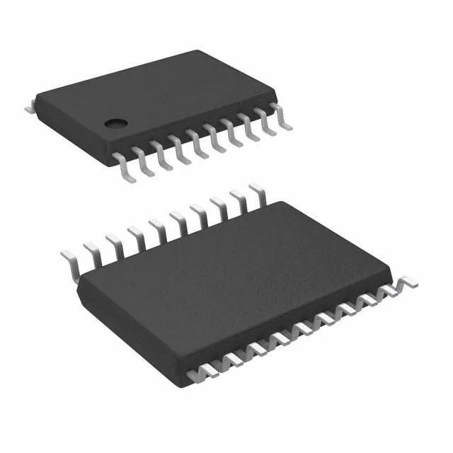
Supply voltage range is 3.135 V to 3.465 V — a tight 3.3 V ±5 % window. The PLL's jitter performance depends on a clean rail; a dedicated LDO or ferrite-bead filter on the 3.3 V plane is standard practice for PCIe clock buffers. Housed in a 20-TSSOP (4.40 mm wide body), surface-mount. The 0.65 mm pin pitch is routable on a standard 4-layer PCIe add-in card or motherboard without micro-vias. Supplied in tube — not tape-and-reel. For automated pick-and-place, confirm the tube-to-reel transfer or request the reel-pack variant if one exists in the family.
Active lifecycle and compliance — no end-of-life risk
ROHS3 compliant (no exemptions).
Sourced through independent distribution channels.