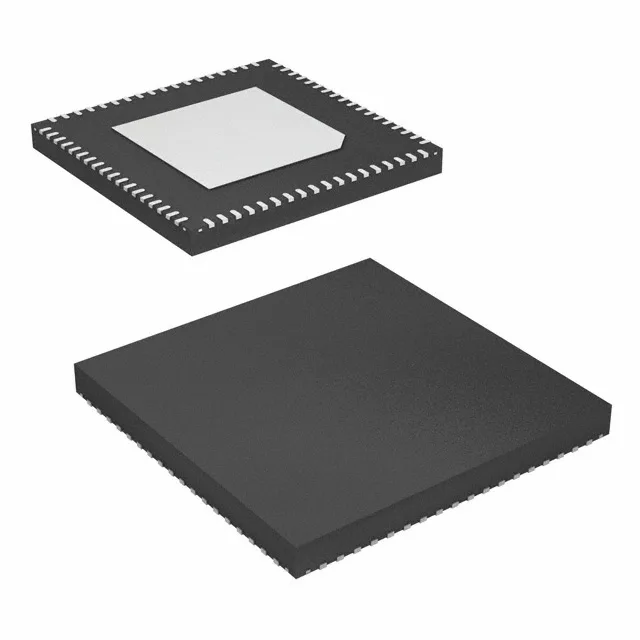
Renesas Electronics 8V41N012NLGI — Clock & Timing ICs

8V41N012NLGI Clock Generator, FemtoClock NG, 312.5MHz

MPN8V41N012NLGI
End of Life

Renesas FemtoClock® NG series, 8V41N012NLGI, Clock Generator, PLL with Bypass, 312.5MHz max, 2:12 input:output, HCSL/LVCMOS/LVDS/LVHSTL/LVPECL/LVTTL/Crystal input, HCSL/LVCMOS/LVTTL output, 3.135V-3.465V supply, -40 to 85°C, 72-VFQFPN (10x10).

$23.33Ref. price · indicative, final on quote
Packaging72-VFQFN Exposed Pad
StockContact for availability
MOQ1 pcs
  • 100% new & originalTraceable channels only — no refurbs, no pulls, no remarked parts.
  • Date & lot codes on quoteStated per line before you commit; label photos on request.
  • MSL-compliant ESD packingMoisture-sealed bags with indicator cards; reels photo-verified.
  • PayPal buyer protectionPay by T/T, PayPal or Payoneer — card payments covered end to end.

Specifications

8V41N012NLGI Technical Specifications
ParameterValue
TypeClock Generator
SeriesFemtoClock® NG
Mounting typeSurface Mount
Voltage3.135V ~ 3.465V
Frequency312.5MHz
Operating temperature-40°C ~ 85°C
PLLYes with Bypass
InputHCSL, LVCMOS, LVDS, LVHSTL, LVPECL, LVTTL, Crystal
OutputHCSL, LVCMOS, LVTTL
PackageTray
Case72-VFQFN Exposed Pad
Divider (Multiplier)Yes/Yes
Number of circuits1
Ratio - Input:Output2:12
Differential - Input:OutputYes/Yes

Product details

What this FemtoClock NG part does on the board

The Renesas 8V41N012NLGI is a clock generator from the FemtoClock® NG series that takes one of several differential or single-ended reference formats — HCSL, LVCMOS, LVDS, LVHSTL, LVPECL, LVTTL, or a crystal — and fans it out to twelve output clocks in HCSL, LVCMOS, or LVTTL levels. The integrated PLL can be bypassed when you need a clean fanout buffer instead of a synthesized frequency. With a maximum output frequency of 312.5 MHz, this part sits in the clock tree for 10G/25G Ethernet switches, wireless base station line cards, and high-speed data-converter reference clocks where jitter budgets are tight and the board needs one device to handle multiple logic families.

2:12 fanout and signal-format flexibility

The 2:12 input-to-output ratio means a single 8V41N012NLGI replaces what might otherwise be a PLL plus a separate fanout buffer, saving board area and reducing the number of crystal oscillators on the bill. The input stage accepts both differential (HCSL, LVDS, LVHSTL, LVPECL) and single-ended (LVCMOS, LVTTL, crystal) references, so the same BOM line works across designs that use a discrete oscillator and designs that take a clock from a backplane or an FPGA. The twelve outputs are individually programmable to HCSL, LVCMOS, or LVTTL, which lets you drive a mix of SerDes reference clocks and lower-speed logic clocks from one device without external level translators.

Industrial temperature and supply tolerance

Rated for -40°C to 85°C operation, the 8V41N012NLGI is specified for outdoor telecom cabinets, factory-floor Ethernet switches, and base stations where the ambient temperature inside the enclosure can climb well above room temperature. The supply range of 3.135 V to 3.465 V gives you ±5% margin around a 3.3 V rail, which is typical for most intermediate-bus converters. If your board runs a 2.5 V or 1.8 V clock section, this part needs a separate 3.3 V rail — it is not a multi-voltage-core device. The 72-VFQFN package with an exposed pad requires a thermal via pattern under the paddle for heat sinking; the datasheet's recommended land pattern is worth following closely because the pad also serves as the ground return for the high-frequency outputs.

Lifecycle and sourcing reality

The 8V41N012NLGI carries an Active product status and ROHS3 compliance. There is no NRND flag, no last-time-buy notice, and no successor part number published — this is a current-production device that qualifies for new designs and production ramps without an obsolescence clock ticking. If you are dual-sourcing a clock generator for a high-volume build, this part is still in the Renesas active portfolio, so the supply channel is stable.

Frequently asked questions

Does the 8V41N012NLGI support a 3.3V supply and 312.5 MHz output?

Yes. The supply range is 3.135 V to 3.465 V, which covers a nominal 3.3 V rail, and the maximum output frequency is 312.5 MHz. The part generates that frequency from the internal PLL or passes through a reference clock when the PLL is bypassed.

Is the 8V41N012NLGI RoHS compliant?

Yes, it is ROHS3 compliant per the lifecycle record.

What are the alternatives or replacements for the 8V41N012NLGI?

The evidence does not list a direct pin-compatible replacement or second-source alternate. Within the FemtoClock NG family, other devices share the same PLL architecture but differ in fanout count, output frequency ceiling, or package. For a drop-in alternate, the Renesas datasheet should be checked for the latest cross-reference table.