Renesas Electronics 8T39S11ANLGI — Clock & Timing ICs

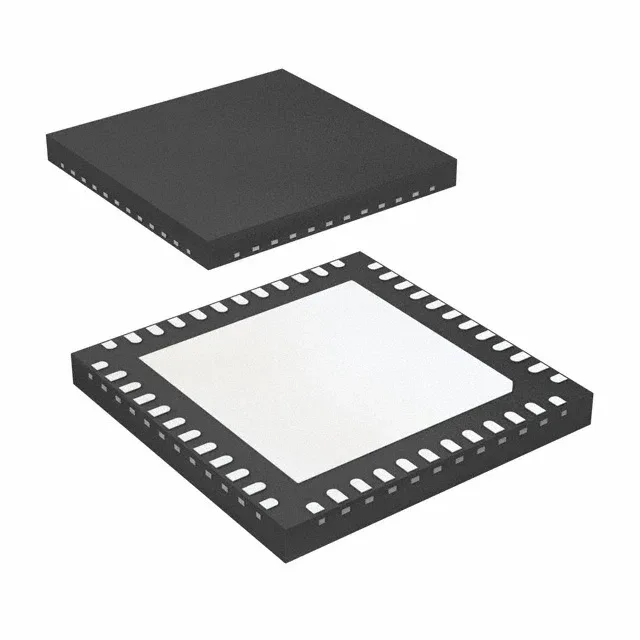
8T39S11ANLGI Renesas Clock Buffer 3:11 2 GHz 48-VFQFN

MPN8T39S11ANLGI
End of Life

Renesas 8T39S11ANLGI, Fanout Buffer (Distribution), Multiplexer, 3:11 input:output ratio, 2 GHz max frequency, differential I/O, 48-VFQFPN (7x7) exposed pad, -40°C to 85°C operation.

$19.77Ref. price · indicative, final on quote
Packaging48-VFQFN Exposed Pad
StockContact for availability
MOQ1 pcs
  • 100% new & originalTraceable channels only — no refurbs, no pulls, no remarked parts.
  • Date & lot codes on quoteStated per line before you commit; label photos on request.
  • MSL-compliant ESD packingMoisture-sealed bags with indicator cards; reels photo-verified.
  • PayPal buyer protectionPay by T/T, PayPal or Payoneer — card payments covered end to end.

Specifications

8T39S11ANLGI Technical Specifications
ParameterValue
TypeFanout Buffer (Distribution), Multiplexer
Mounting typeSurface Mount
Voltage2.375V ~ 3.465V
Frequency2 GHz
Operating temperature-40°C ~ 85°C
InputHCSL, HSTL, LVDS, LVPECL, Crystal
OutputHCSL, LVDS, LVPECL
PackageTray
Case48-VFQFN Exposed Pad
Number of circuits1
Ratio - Input:Output3:11
Differential - Input:OutputYes/Yes

Product details

3:11 fanout buffer with multiplexer — what the ratio buys

The 8T39S11ANLGI is a 3:11 fanout buffer with an integrated multiplexer — three input sources (HCSL, HSTL, LVDS, LVPECL, or a crystal) are selectable, and the selected clock is fanned out to eleven differential outputs (HCSL, LVDS, or LVPECL). The 3:11 ratio is the key parametric: it replaces a separate mux plus a multi-output fanout tree, saving board space and reducing additive jitter from cascaded buffers. The 2 GHz max frequency covers PCIe Gen4/5 reference clocks, 10GbE, Fibre Channel, and 100G backplane distributions. The differential input and output path keeps signal integrity clean across the fanout tree — single-ended clocking would limit reach and noise margin at these speeds.

Supply range and temperature grade — board-level fit

Supply voltage spans 2.375 V to 3.465 V, covering both 2.5 V and 3.3 V rails without an extra regulator.

Active production — no obsolescence pressure

The BOM line can be committed without an obsolescence risk flag — sourced per RFQ against the required quantity.

Frequently asked questions

Is 8T39S11ANLGI compatible with HCSL outputs?

Yes — the outputs are configurable as HCSL, LVDS, or LVPECL. HCSL is the common choice for PCIe reference clocks; LVDS suits backplane distribution; LVPECL is typical in high-speed serial links.

Is 8T39S11ANLGI compatible with LVPECL inputs?

Yes — the input stage accepts LVPECL, along with HCSL, HSTL, LVDS, and a crystal. The crystal input allows a local oscillator to be the clock source without an external XO buffer.

What are the direct alternatives for 8T39S11ANLGI?

The closest functional sibling in the same family is the 8SLVP1204ANLGI8 — a 2:4 fanout buffer with LVPECL outputs, also 2 GHz, same supply range (2.375 V), same temperature grade. The 8T39S11ANLGI offers a 3:11 ratio with multiplexer and three output types (HCSL/LVDS/LVPECL) versus the 8SLVP1204's 2:4 ratio and LVPECL-only output. If your design needs more than four outputs or multiple output standards, the 8T39S11ANLGI is the fit.