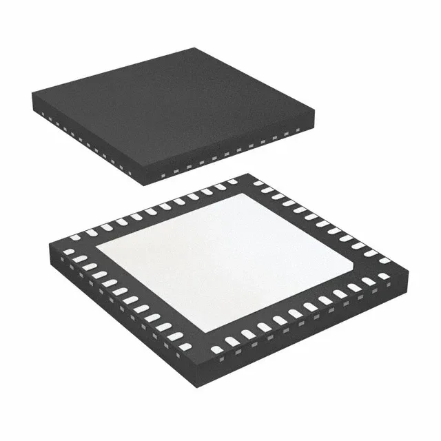
2 GHz fanout buffer with 3:5 mux — what the ratings mean for your clock tree
The 8T39S04ANBGI8 is a Renesas fanout buffer with an integrated multiplexer, rated for clock distribution up to 2 GHz. The 3:5 input-to-output ratio means three selectable clock sources feed five output lanes — useful for redundant clock architectures where a single PLL or oscillator failure switches to a backup without board-level rework. All signal paths are fully differential (input and output), which preserves the rise-time integrity and common-mode rejection needed at 2 GHz. The 2 GHz ceiling covers 10GbE reference clocks, 100G SerDes, and FPGA transceiver reference frequencies — the buffer itself does not limit the lane rate.
Input and output standards — one buffer for mixed-logic clock domains
The input stage accepts HCSL, HSTL, LVDS, LVPECL, and crystal sources — five common clock formats without external level translation. On a typical board, the reference oscillator might be LVDS, the FPGA PLL output is LVPECL, and the downstream SerDes expects HCSL; this buffer handles all three on the same die. Outputs are available in HCSL, LVDS, or LVPECL, matching the most common high-speed interconnect standards. The output swing and common-mode voltage are set by the supply rail — 2.5V or 3.3V — so the buffer aligns with the receiver's input threshold without AC-coupling caps in many cases.
Supply voltage and temperature — two rails, one industrial grade
The device operates from either a 2.375V to 2.625V rail or a 3.135V to 3.465V rail.
Active production, ROHS3, and sourcing posture
Renesas lists the 8T39S04ANBGI8 as active with ROHS3 compliance. No stock-holding claim — quoted to order per RFQ.