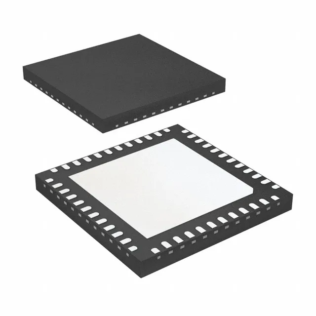
1:8 LVPECL fanout at 2 GHz — what this buffer does on the board
The Renesas 8SLVP2108ANLGI/W is a 1:8 fanout buffer that takes a single differential or single-ended clock input — CML, LVCMOS, LVDS, or LVPECL — and delivers eight LVPECL copies at up to 2 GHz. Supply range spans 2.375 V to 3.465 V. The 48-VFQFPN package with exposed pad pulls heat into the ground plane.
Input flexibility and output standard — one buffer, multiple signal types
The input accepts CML, LVCMOS, LVDS, and LVPECL. That means the same BOM line works whether the source is an FPGA with LVDS outputs, an oscillator in LVPECL, or a serdes in CML. No level-shifting resistors or translator ICs between the source and this buffer.
Operating range — industrial temperature, no surprises
No extended-temperature derating needed for typical infrastructure gear. Two independent buffer circuits share the package — each with its own input and eight outputs. That lets you distribute two unrelated clock domains from one IC, saving board area versus two separate buffers.
ROHS3 compliant.