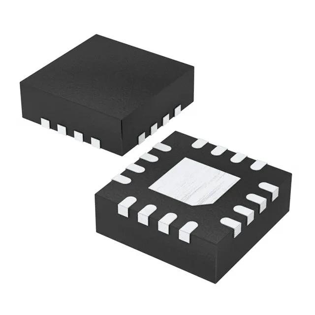
Renesas Electronics 8SLVP2106ANLGI — Clock & Timing ICs

8SLVP2106ANLGI Fanout Buffer, 2 GHz, 1:6, LVPECL, 16-VFQFN

MPN8SLVP2106ANLGI
End of Life

Renesas 8SLVP2106ANLGI, Fanout Buffer (Distribution), 2 circuits, 1:6 input:output, 2 GHz max frequency, LVPECL output, 16-VFQFN (3x3 mm) exposed pad, -40 to 85°C, 2.375V to 3.465V supply.

$11.2Ref. price · indicative, final on quote
Packaging16-VFQFN Exposed Pad
StockContact for availability
MOQ1 pcs
  • 100% new & originalTraceable channels only — no refurbs, no pulls, no remarked parts.
  • Date & lot codes on quoteStated per line before you commit; label photos on request.
  • MSL-compliant ESD packingMoisture-sealed bags with indicator cards; reels photo-verified.
  • PayPal buyer protectionPay by T/T, PayPal or Payoneer — card payments covered end to end.

Specifications

8SLVP2106ANLGI Technical Specifications
ParameterValue
TypeFanout Buffer (Distribution)
Mounting typeSurface Mount
Voltage2.375V ~ 3.465V
Frequency2 GHz
Operating temperature-40°C ~ 85°C
InputCML, LVCMOS, LVDS, LVPECL
OutputLVPECL
PackageTray
Case16-VFQFN Exposed Pad
Number of circuits2
Ratio - Input:Output1:6
Differential - Input:OutputYes/Yes

Product details

2 GHz fanout buffer with multi-standard input flexibility

The Renesas 8SLVP2106ANLGI is a 2-circuit fanout buffer that accepts CML, LVCMOS, LVDS, or LVPECL inputs and delivers LVPECL outputs at frequencies up to 2 GHz. Each of the two buffer circuits provides a 1:6 fanout, giving you 12 total outputs from two input lanes. This makes it a strong fit for high-speed clock distribution in telecom, data center, and test equipment where you need to split a clean reference clock across multiple ASICs, FPGAs, or SerDes transceivers without adding jitter.

What the 2 GHz rating means for your clock tree

The 2 GHz max frequency covers the common high-speed clock rates used in 10 GbE, 100G/400G line cards, and RF sampling converters. At these frequencies, signal integrity depends on keeping the trace impedance matched and the propagation delay skew low. The differential input and output (both rated yes) help reject common-mode noise on long board traces. The 1:6 fanout per circuit means one clean PLL output can feed six receiver loads — enough for a typical multi-FPGA board without adding a second buffer stage.

Supply voltage range and temperature grade

The part operates from 2.375 V to 3.465 V, covering 2.5 V and 3.3 V nominal rails with margin for ripple. The industrial temperature range of -40°C to 85°C suits outdoor telecom cabinets and base stations where ambient temperatures swing. The 16-VFQFN with exposed pad (3x3 mm) needs a thermal via array under the paddle to pull heat into the ground plane — without it, junction temperature climbs faster than the datasheet derating curve suggests at high fanout and 2 GHz.

Active lifecycle — no LTB risk

The 8SLVP2106ANLGI carries an Active lifecycle status per Renesas. For new designs this means you can qualify it without worrying about an EOL notice mid-cycle. The ROHS3 compliance is confirmed.

Sourcing and availability

This part is sourced through independent distribution channels and is quoted to order against an RFQ. For BOM planning, the active status and multi-standard input flexibility reduce the risk of a single-source bottleneck — if you need a second source, the 8SLVP2108ANLGI/W offers the same 2 GHz performance with a 1:8 fanout per circuit in a similar package.

Frequently asked questions

Does 8SLVP2106ANLGI support CML input?

Yes, the input stage accepts CML, LVCMOS, LVDS, and LVPECL signal levels, so you can feed it directly from a CML clock source without external level translation.

Is 8SLVP2106ANLGI equivalent to 8SLVP2106NLG?

The 8SLVP2106NLG suffix typically indicates a different packaging or tape/reel option. The functional specifications (2 GHz, 1:6, LVPECL) are the same. Confirm the exact order code with your distributor to match your BOM.