The Renesas 8SLVP1104ANLGI is a 1:4 fanout buffer that takes a single differential clock input — CML, LVDS, or LVPECL — and delivers four LVPECL outputs at up to 2 GHz. It's built for high-speed serial clock trees where the edge rate and jitter budget are tight. The 3.135 V to 3.465 V supply rail and industrial temperature range (-40°C to 85°C) let it sit on a line card or in outdoor telecom gear without a second regulator.
If you need a higher fanout or a different output family, the 8SLVP2108ANLGI/W is a 1:8 LVPECL buffer on the same process — same 2 GHz ceiling, same supply range, but two banks of four outputs.
Package and mounting — 16-VFQFPN with exposed pad
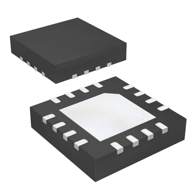
The 8SLVP1104ANLGI comes in a 16-lead VFQFPN with an exposed pad (3 mm x 3 mm). Surface-mount only. No through-hole option, so factor that into a prototype or rework plan. The tube shipment is fine for bench builds; production volumes will typically move to tape-and-reel (check the -/W suffix variant for that).