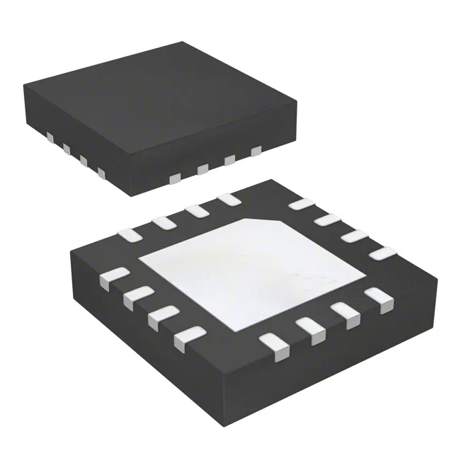
Renesas Electronics 8SLVD2102NLGI — Clock & Timing ICs

8SLVD2102NLGI 2 GHz LVDS Fanout Buffer

MPN8SLVD2102NLGI
End of Life

Renesas Electronics 8SLVD2102NLGI, Fanout Buffer (Distribution), 2:4 LVDS, 2 GHz max, 2.375V–2.625V supply, 16-VFQFPN (3x3), -40°C to 85°C, tray.

$6.49Ref. price · indicative, final on quote
Packaging16-VFQFN Exposed Pad
RoHSROHS3 Compliant
Independent supplier — new & surplus stockAuthenticity-screened · ESD-safe packingListing updated Aug 2026

Specifications

8SLVD2102NLGI specifications
ParameterValue
TypeFanout Buffer (Distribution)
MountingSurface Mount
Voltage2.375V ~ 2.625V
Frequency2 GHz
Operating temperature-40°C ~ 85°C (TA)
InputLVDS, LVPECL
OutputLVDS
PackageTray
Case16-VFQFN Exposed Pad
Number of circuits2
Ratio - Input:Output2:4
Differential - Input:OutputYes/Yes

Product details

2 GHz LVDS fanout — where the 2:4 ratio fits

The 8SLVD2102NLGI is a 2:4 differential fanout buffer from Renesas, accepting LVDS or LVPECL inputs and delivering LVDS outputs at frequencies up to 2 GHz. The 2:4 ratio means two input channels each fan out to two outputs — useful for splitting a reference clock to multiple SERDES transceivers or FPGA banks without adding separate PLLs. The 2.375V to 2.625V supply range centres on 2.5V. If your board already has a 2.5V supply for the FPGA transceiver bank, this buffer can share it.

Supply rail and temperature grade — BOM-fit checks

Compared to the LVPECL-output sibling 8SLVP1104ANLGI (1:4, 3.135V supply), the 8SLVD2102NLGI runs on a lower 2.5V rail and outputs LVDS, which consumes less power and simplifies termination — no pull-up resistors to VCC-2V. The 8SLVP1204ANLGI8 adds a multiplexer function but still outputs LVPECL. For a pure LVDS fanout at 2 GHz, this is the direct fit.

Frequently asked questions

Does the 8SLVD2102NLGI work with a 2.5V supply?

Yes — the supply voltage range is 2.375V to 2.625V, which centres on 2.5V. The buffer expects a clean 2.5V rail; do not share a 3.3V or 1.8V plane without a regulator.