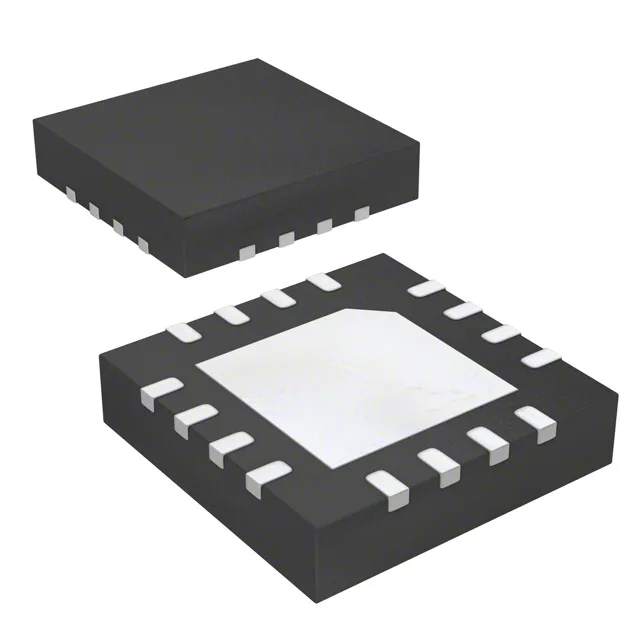
Renesas Electronics 8S89833AKILF — Clock & Timing ICs

Renesas 8S89833AKILF Fanout Buffer, 1:4, 2 GHz, LVDS

MPN8S89833AKILF
End of Life

Renesas Electronics 8S89833AKILF Fanout Buffer (Distribution), 1:4 LVDS output, 2 GHz max, CML/LVDS/LVPECL input, 16-VFQFPN (3x3) surface-mount, tray.

$7.84Ref. price · indicative, final on quote
Packaging16-VFQFN Exposed Pad
StockContact for availability
Lead timeIn Stock wk
MOQ1 pcs
  • 100% new & originalTraceable channels only — no refurbs, no pulls, no remarked parts.
  • Date & lot codes on quoteStated per line before you commit; label photos on request.
  • MSL-compliant ESD packingMoisture-sealed bags with indicator cards; reels photo-verified.
  • PayPal buyer protectionPay by T/T, PayPal or Payoneer — card payments covered end to end.

Specifications

8S89833AKILF Technical Specifications
ParameterValue
TypeFanout Buffer (Distribution)
Mounting typeSurface Mount
Voltage3V ~ 3.6V
Frequency2 GHz
Operating temperature-40°C ~ 85°C
InputCML, LVDS, LVPECL
OutputLVDS
PackageTray
Case16-VFQFN Exposed Pad
Number of circuits1
Ratio - Input:Output1:4
Differential - Input:OutputYes/Yes

Product details

2 GHz fanout buffer for high-speed clock distribution

The 8S89833AKILF is a 1:4 fanout buffer from Renesas, designed to distribute a single differential clock input to four LVDS outputs with a maximum frequency of 2 GHz. This makes it suitable for clock-tree fanout in high-speed data converter, FPGA reference clock, and SerDes applications where signal integrity at multi-gigahertz rates is critical.

Signal standard and supply rail compatibility

The input stage accepts CML, LVDS, or LVPECL levels, while the outputs are LVDS — a common pairing that keeps the signal swing differential and the common-mode voltage within the receiver's input range without external level shifting. The supply voltage spans 3 V to 3.6 V, which aligns with standard 3.3 V clock-distribution rails. With a differential input-to-output path (Yes/Yes per the spec), the buffer preserves the low-jitter characteristics of the incoming clock. The single-circuit, 1:4 ratio means one input drives four copies — useful for fanning a master clock to multiple ADCs, FPGAs, or SerDes transceivers on the same board.

Package, footprint, and reflow considerations

Housed in a 16-VFQFN exposed-pad package (3x3 mm body, supplier device package 16-VFQFPN), the part sits on a 0.5 mm pitch land pattern. The small footprint means the buffer fits into dense clock trees where board real estate is tight.

Active lifecycle and compliance status

No end-of-life notice or successor is recorded — the part is current-production and suitable for both new designs and ongoing BOM replenishment.

Frequently asked questions

What is the 8S89833AKILF used for?

The 8S89833AKILF is a 1:4 fanout buffer that distributes one differential clock input (CML, LVDS, or LVPECL) to four LVDS outputs at up to 2 GHz. It is used in high-speed clock distribution for ADCs, DACs, FPGAs, and SerDes interfaces where multiple devices need a synchronized, low-jitter reference clock.

How does the 8S89833AKILF compare to the 8SLVP1104ANLGI?

Both are 1:4 fanout buffers with 2 GHz max frequency and accept CML, LVDS, or LVPECL inputs. The key difference is the output standard: the 8S89833AKILF outputs LVDS, while the 8SLVP1104ANLGI outputs LVPECL. The choice depends on the receiver — LVDS is lower power and common for FPGA clock inputs, while LVPECL has a larger swing and is preferred for long backplane traces. The packages differ as well: the 8S89833AKILF is in a 16-VFQFPN (3x3 mm), while the 8SLVP1104ANLGI comes in a different package. They are not pin-compatible drop-in replacements.