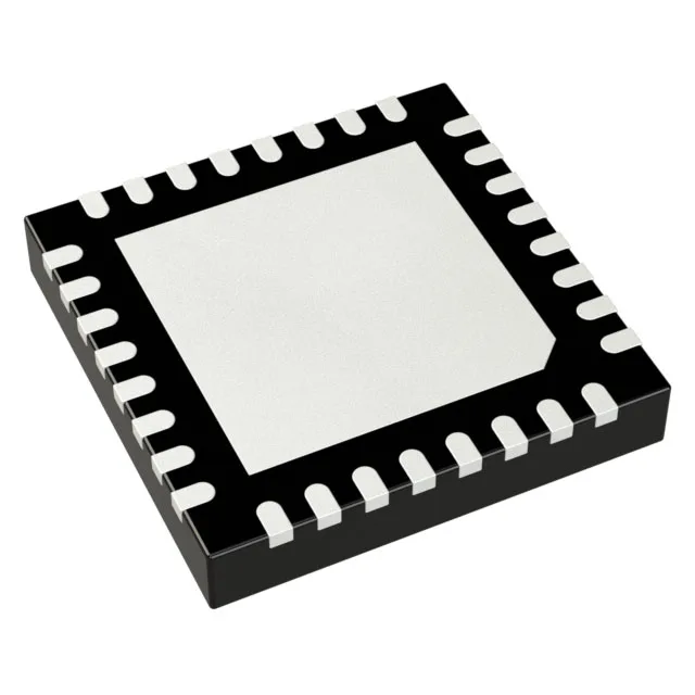
Renesas Electronics 853S12AKILF — Clock & Timing ICs

Renesas 853S12AKILF Fanout Buffer, 1:12, 1.5 GHz

MPN853S12AKILF
End of Life

Renesas Electronics 853S12AKILF Fanout Buffer (Distribution), 1:12 ratio, 1.5 GHz max, LVPECL output, CML/LVPECL/SSTL input, 32-VFQFN Exposed Pad, Tray.

$35.01Ref. price · indicative, final on quote
Packaging32-VFQFN Exposed Pad
StockContact for availability
Lead timeIn Stock wk
MOQ1 pcs
  • 100% new & originalTraceable channels only — no refurbs, no pulls, no remarked parts.
  • Date & lot codes on quoteStated per line before you commit; label photos on request.
  • MSL-compliant ESD packingMoisture-sealed bags with indicator cards; reels photo-verified.
  • PayPal buyer protectionPay by T/T, PayPal or Payoneer — card payments covered end to end.

Specifications

853S12AKILF Technical Specifications
ParameterValue
TypeFanout Buffer (Distribution)
Mounting typeSurface Mount
Voltage2.375V ~ 3.465V
Frequency1.5 GHz
Operating temperature-40°C ~ 85°C
InputCML, LVPECL, SSTL
OutputLVPECL
PackageTray
Case32-VFQFN Exposed Pad
Number of circuits1
Ratio - Input:Output1:12
Differential - Input:OutputYes/Yes

Product details

What the 1:12 fanout and 1.5 GHz ceiling mean for your clock tree

The 853S12AKILF is a 1:12 fanout buffer — one differential input gets split into twelve identical LVPECL outputs. That ratio matters when you have a single high-frequency reference (say, from an oscillator or PLL) that needs to drive multiple downstream devices like SERDES, FPGAs, or ADCs without loading the source. Rated for 1.5 GHz maximum frequency, this buffer handles common telecom and data-center clock rates including 156.25 MHz, 312.5 MHz, and 625 MHz with margin. The differential input accepts CML, LVPECL, or SSTL levels, so it sits between a wide range of clock sources and the LVPECL fanout tree.

Supply range, temperature grade, and signal integrity

The wide tolerance means you can run it off a 3.3 V supply that droops under load and still stay within spec. The 32-VFQFPN (5x5 mm) exposed-pad package helps pull heat out of the die when the buffer is driving twelve 50-ohm terminated lines at full rate. Differential input and output paths (Yes/Yes per the spec) reject common-mode noise on the clock lines — critical when routing high-speed clocks across a board with switching regulators or digital busses nearby.

Listed as Active by Renesas with ROHS3 compliance. Supplied in tray packaging, surface-mount to a 32-VFQFN exposed-pad footprint.

Frequently asked questions

What input signal types does 853S12AKILF accept?

It accepts CML, LVPECL, and SSTL differential inputs. That covers the three most common high-speed clock signaling families, so it can buffer from a wide range of oscillators, PLLs, or clock generators.

How does 853S12AKILF compare to the 8SLVP1104ANLGI?

The 8SLVP1104ANLGI is a 1:4 fanout buffer with a 2 GHz ceiling, while the 853S12AKILF provides a 1:12 fanout at 1.5 GHz. If your design needs twelve outputs instead of four, the 853S12AKILF saves a second buffer stage. Both run on LVPECL outputs and accept CML/LVPECL inputs, but the 8SLVP1104 also accepts LVDS inputs.