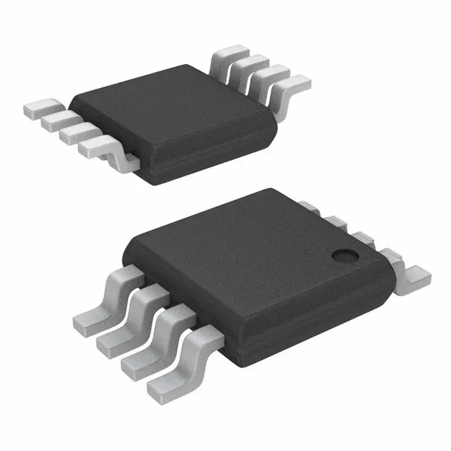
1:2 fanout buffer for 2.5 GHz clock distribution
The Renesas 853S011BGILF is a 1:2 fanout buffer in an 8-TSSOP package, designed to distribute a single differential clock input to two differential output paths at frequencies up to 2.5 GHz. The 1:2 ratio means one input drives two outputs with minimal additive jitter — critical for splitting a reference clock to multiple PLLs or SerDes transceivers without degrading the timing budget.
Differential I/O and supply rail flexibility
Differential input accepts CML, LVDS, LVPECL, or SSTL signal levels, while the outputs drive ECL or LVPECL loads — the buffer handles the level translation internally, so the input standard does not have to match the output standard. The wide range also allows the buffer to sit on a shared 3.3 V plane while the core logic runs at 2.5 V.
For new designs, the active status means no last-time-buy risk during the product lifecycle.