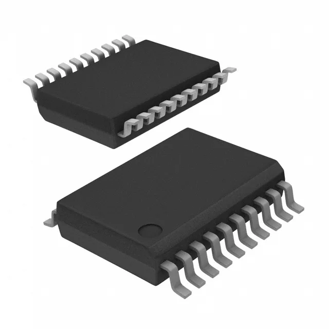
Renesas Electronics 74FCT3807AQG — Clock & Timing ICs

74FCT3807AQG Fanout Buffer, 1:10, 100 MHz, 20-QSOP

MPN74FCT3807AQG
End of Life

Renesas 74FCT3807AQG, 74FCT series, Fanout Buffer (Distribution), 1:10, 100 MHz, LVTTL input, CMOS/TTL output, 3V–3.6V supply, 20-QSOP, 0°C to 70°C.

$1.47Ref. price · indicative, final on quote
Packaging20-SSOP (0.154", 3.90mm Width)
StockContact for availability
MOQ1 pcs
  • 100% new & originalTraceable channels only — no refurbs, no pulls, no remarked parts.
  • Date & lot codes on quoteStated per line before you commit; label photos on request.
  • MSL-compliant ESD packingMoisture-sealed bags with indicator cards; reels photo-verified.
  • PayPal buyer protectionPay by T/T, PayPal or Payoneer — card payments covered end to end.

Specifications

74FCT3807AQG Technical Specifications
ParameterValue
TypeFanout Buffer (Distribution)
Series74FCT
Mounting typeSurface Mount
Voltage3V ~ 3.6V
Frequency100 MHz
Operating temperature0°C ~ 70°C
InputLVTTL
OutputCMOS, TTL
PackageTube
Case20-SSOP (0.154\", 3.90mm Width)
Number of circuits1
Ratio - Input:Output1:10
Differential - Input:OutputNo/No

Product details

What this 1:10 fanout buffer does on your board

The Renesas 74FCT3807AQG is a single-circuit fanout buffer that takes one LVTTL clock or signal input and distributes it to ten CMOS/TTL outputs, each capable of running up to 100 MHz. It operates from a 3V to 3.6V supply. The part is housed in a 20-QSOP — a narrow-body surface-mount package. It is rated for commercial temperature range (0°C to 70°C).

Why the 1:10 ratio and 100 MHz matter for your BOM

The 1:10 fanout means a single clock source can drive up to ten loads. The 100 MHz ceiling is the maximum toggle rate.

Lifecycle and sourcing posture

It is ROHS3 compliant, which covers the latest EU restriction requirements. For BOM planning, this part is a safe choice for new designs and ongoing production — no near-term end-of-life risk.

Package rework and board-fit notes

The 20-QSOP (0.154-inch body width, 3.90 mm) is a fine-pitch SSOP variant. The narrow body means it takes less board space than a wide SOIC, but the pad spacing is tight enough that a good flux and controlled reflow profile matter. If you are hand-reworking, preheat the board to 100°C to avoid lifting the small pads. The part is surface-mount only; no through-hole option exists.

Frequently asked questions

Is 74FCT3807AQG compatible with 3.3V?

Yes, the 74FCT3807AQG operates from a 3V to 3.6V supply, which directly covers the 3.3V logic rail. The LVTTL input and CMOS/TTL outputs are 3.3V-compatible without any level shifting.

Does 74FCT3807AQG support differential inputs?

No, the 74FCT3807AQG has non-differential inputs and outputs (LVTTL in, CMOS/TTL out). For differential clock distribution (e.g., LVPECL, LVDS), consider a part like the 8SLVP1104ANLGI, which accepts differential signals and provides LVPECL outputs.

What is the equivalent or second-source for 74FCT3807AQG?

There is no direct pin-compatible second-source listed in the official records. The closest functional peer in the same fanout-buffer class is the 8SLVP1104ANLGI, but that part is differential (LVPECL) and operates at 2 GHz — a different performance tier and signal type. For a drop-in replacement, stick with the 74FCT3807AQG.