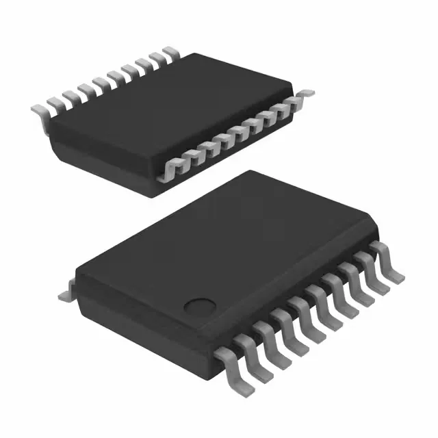
Renesas Electronics 74FCT3807APYG — Clock & Timing ICs

74FCT3807APYG Fanout Buffer, 1:10, 100 MHz, 20-SSOP

MPN74FCT3807APYG
End of Life

Renesas 74FCT3807APYG, 74FCT series Fanout Buffer (Distribution), 1:10, LVTTL input, CMOS/TTL output, 100 MHz max, 3V-3.6V supply, 20-SSOP, 0°C to 70°C.

$1.54Ref. price · indicative, final on quote
Packaging20-SSOP (0.209", 5.30mm Width)
StockContact for availability
MOQ1 pcs
  • 100% new & originalTraceable channels only — no refurbs, no pulls, no remarked parts.
  • Date & lot codes on quoteStated per line before you commit; label photos on request.
  • MSL-compliant ESD packingMoisture-sealed bags with indicator cards; reels photo-verified.
  • PayPal buyer protectionPay by T/T, PayPal or Payoneer — card payments covered end to end.

Specifications

74FCT3807APYG Technical Specifications
ParameterValue
TypeFanout Buffer (Distribution)
Series74FCT
Mounting typeSurface Mount
Voltage3V ~ 3.6V
Frequency100 MHz
Operating temperature0°C ~ 70°C
InputLVTTL
OutputCMOS, TTL
PackageTube
Case20-SSOP (0.209\", 5.30mm Width)
Number of circuits1
Ratio - Input:Output1:10
Differential - Input:OutputNo/No

Product details

100 MHz fanout buffer with 1:10 distribution

The Renesas 74FCT3807APYG is a single-circuit fanout buffer that takes one LVTTL input and distributes it to ten CMOS or TTL outputs, running at a maximum frequency of 100 MHz. It operates from a 3V to 3.6V supply and comes in a 20-SSOP surface-mount package. This is a commercial-temperature-grade part (0°C to 70°C), suited for indoor equipment like servers, telecom line cards, and test instrumentation where a clean, non-differential clock fanout is needed.

1:10 fanout — BOM density per clock tree

The 1:10 input-to-output ratio is the key density spec. One 74FCT3807APYG replaces two 1:4 or 1:5 buffers, saving board area and reducing the number of clock-tree stages. The non-differential topology (No/No for differential input/output) means it is a straight single-ended buffer — no PECL or CML translation needed, which simplifies the layout for 3.3V CMOS clock distribution.

3.3V supply rail — what it means for the power design

The supply range is 3V to 3.6V, which is essentially a 3.3V ±10% rail. This buffer will not run from a 2.5V or 5V supply without a regulator. On a mixed-voltage board, allocate a dedicated 3.3V rail or a local LDO for this device to keep the clock buffer supply clean — switching noise on the supply rail couples into the output jitter.

Commercial temperature grade — deployment boundary

Rated for 0°C to 70°C, this part is limited to indoor, temperature-controlled environments.

Active lifecycle — no end-of-life pressure

ROHS3 compliance is confirmed.

Frequently asked questions

What is the maximum frequency of the 74FCT3807APYG?

The 74FCT3807APYG is rated for a maximum frequency of 100 MHz. This is a single-ended, non-differential buffer, so it is not suited for high-speed differential clocks above that ceiling.