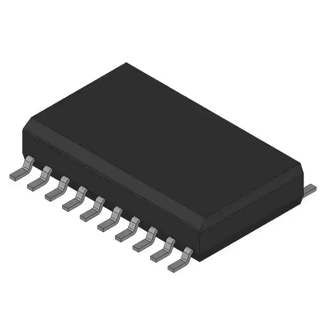
Timing and drive for the 5V data path
The 74FCT374CTSOG8 is an 8-bit D-type flip-flop from the 74FCT series, capturing data on the positive clock edge and presenting it through tri-state, non-inverted outputs. Maximum propagation delay of 5.2 ns at 5 V with a 50 pF load sets the timing budget for the data path — at a 100 MHz clock the output must settle within half a period, so this delay plus the upstream logic's clock-to-Q and routing skew must sum to under 5 ns for zero hold-time margin. The output stage sources 15 mA and sinks 48 mA, enough to drive a heavily loaded bus or a bank of LED indicators without external buffers.
Supply and temperature envelope
Quiescent current draw is 1 mA typical — negligible in a mixed-signal board where the power budget is dominated by the processor or ADC.
Board-fit and signal-integrity parameters
Input capacitance is 6 pF per pin — a modest load on the driving gate, though the cumulative bus load of eight parallel inputs plus trace capacitance must stay within the driver's fan-out spec. Surface-mount assembly with MSL level typical for SOIC packages; no special bake required before reflow if stored in dry conditions.