Package and board integration
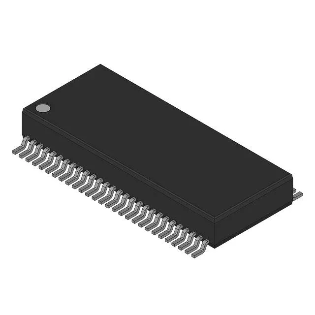
The 74FCT162823ATPVG comes in a 56-BSSOP (0.295", 7.50mm width) package, with the supplier device package designated as 56-SSOP. The 0.65 mm typical lead pitch demands a controlled impedance trace width for the nine-bit-wide data bus on each element.
Supply voltage and timing budget
The 20 ns maximum propagation delay at 5 V with a 300 pF load sets the bus timing ceiling — budget this into the clock-to-output path for a 50 MHz bus, where the 20 ns delay leaves 10 ns of margin per half-cycle before setup time constraints.
Output drive and signal integrity
Tri-state non-inverted outputs source and sink 24 mA each, which is sufficient to drive a 50 pF bus load at 5 V with a 3 ns rise time. The 3.5 pF input capacitance keeps the fan-out per driven gate at 10 standard 74FCT loads without exceeding the output current limit.
Temperature grade and quiescent draw
Quiescent current is 500 µA typical — the static power draw at 5 V is 2.5 mW, negligible in a mixed-signal system but worth noting for battery-backed retention scenarios.