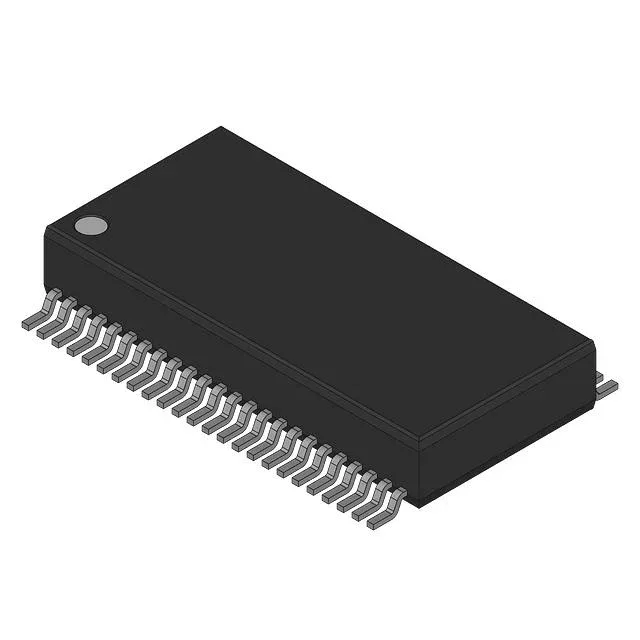
Renesas Electronics 74FCT162374ETPVG — Analog & Data Acquisition

Renesas 74FCT162374ETPVG D-Type Flip-Flop, 3.7ns, 48-SSOP

MPN74FCT162374ETPVG
End of Life

Renesas Electronics 74FCT series D-Type flip-flop, 74FCT162374ETPVG, dual 8-bit, positive edge triggered, tri-state non-inverted outputs, 48-BSSOP, 4.5V-5.5V, -40°C to 85°C.

$2.01Ref. price · indicative, final on quote
Packaging48-BSSOP (0.295", 7.50mm Width)
Series74FCT
Sourced new & surplus through independent channelsAuthenticity-screened · ESD-safe packingListing updated Aug 2026

Specifications

74FCT162374ETPVG specifications
ParameterValue
TypeD-Type
Series74FCT
Output typeTri-State, Non-Inverted
Trigger typePositive Edge
MountingSurface Mount
Voltage4.5V ~ 5.5V
Current - quiescent500 µA
Current - output high, low24mA, 24mA
Operating temperature-40°C ~ 85°C (TA)
PackageBulk
FunctionStandard
Case48-BSSOP (0.295\", 7.50mm Width)
Input capacitance3.5 pF
Number of elements2
Number of bits per element8
Max propagation delay @ v, max CL3.7ns @ 5V, 50pF

Product details

3.7 ns propagation delay — what it means for bus timing

The 74FCT162374ETPVG is a dual 8-bit D-type flip-flop from the 74FCT series, clocked on the positive edge with non-inverting tri-state outputs. Its 3.7 ns max propagation delay at 5 V and 50 pF load sets the data-to-output settling window — for a 50 MHz bus cycle (20 ns period), the output is valid within 18.5% of the cycle, leaving 16.3 ns for setup and hold at the receiver. This margin matters when the part sits in a fan-out buffer or pipeline register driving multiple loads. The 24 mA symmetrical output drive (both high and low) drives the specified 50 pF load without edge-rate degradation. On a heavily loaded backplane, the actual rise time depends on the total capacitance; the 3.5 pF input capacitance per channel keeps the loading on the driving stage low.

The 500 µA quiescent current is the standby draw when all outputs are static — the dynamic current scales with the clock frequency and output load, not this figure. The 48-BSSOP package (7.50 mm body width) is a standard SSOP footprint — board layout matches the JEDEC MO-118 variation.

Active lifecycle — no end-of-life concern

Renesas lists the 74FCT162374ETPVG as Active — no PCN, no last-time-buy window, no successor to track.

Frequently asked questions

What is the propagation delay of the 74FCT162374ETPVG?

This is the tPD from clock edge to data output valid — the spec that governs the maximum clock frequency in a synchronous bus design.