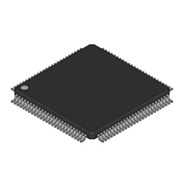
Renesas Electronics 71V547S100PFG — DC-DC Power Modules

71V547S100PFG SRAM, 4.5 Mbit, 10 ns, 100-TQFP

MPN71V547S100PFG
End of Life

Renesas 71V547S100PFG synchronous SRAM, SDR (ZBT), 4.5 Mbit organized 128K x 36, 10 ns access time, parallel interface, 3.135 V to 3.465 V supply, 0°C to 70°C, 100-TQFP.

$3.84Ref. price · indicative, final on quote
Packaging100-LQFP
Independent supplier — new & surplus stockAuthenticity-screened · ESD-safe packingListing updated Jul 2026

Specifications

71V547S100PFG specifications
ParameterValue
Memory typeVolatile
MountingSurface Mount
Voltage3.135V ~ 3.465V
Memory interfaceParallel
Operating temperature0°C ~ 70°C (TA)
PackageBulk
TechnologySRAM - Synchronous, SDR (ZBT)
Access time10 ns
Memory size4.5Mbit
Memory formatSRAM
Case100-LQFP
Memory organization128K x 36

Product details

4.5 Mbit synchronous ZBT SRAM — 10 ns access, 128K x 36 organization

The Renesas 71V547S100PFG is a 4.5 Mbit synchronous SRAM with a Zero Bus Turnaround (ZBT) architecture, organized as 128K words by 36 bits. The 10 ns access time supports bus operation at clock rates up to 100 MHz without wait states in most single-cycle read/write sequences. The 36-bit word width is a natural fit for systems that carry parity or ECC alongside a 32-bit datapath — common in network switches, base stations, and telecom line cards where data integrity matters.

Supply and temperature — design-in constraints

The supply range is 3.135 V to 3.465 V, a tight ±5% window around the nominal 3.3 V rail. That means the board's 3.3 V regulator needs to hold regulation within that band under load — a standard 3.3 V ±5% rail is fine, but a rail that droops to 3.0 V during transient events will violate the minimum. This part is not rated for industrial enclosures, outdoor cabinets, or under-hood environments. If your system sees -20°C or +85°C ambient, this is not the SRAM for that BOM.

Housed in a 100-pin LQFP (supplier device package 100-TQFP, 14x14 mm body). Keep the decoupling capacitors close to the supply pins; the synchronous switching edges draw transient currents that need a low-inductance path.

Frequently asked questions

What is the exact memory size and organization of 71V547S100PFG?

The memory size is 4.5 Mbit, organized as 128K words by 36 bits. That 36-bit width is wider than the common x8 or x16 SRAM, making it suited for systems that need parity or ECC alongside a 32-bit data bus.

What is the access time of 71V547S100PFG?

The access time is 10 ns. At a 100 MHz bus clock, that allows single-cycle read/write operations without wait states in most cases, assuming the controller's output hold and setup times are within the SRAM's timing window.