Active production, industrial temp range
The 71V3579S80PFGI: Organised 256K x 18, the extra two bits per word are useful for parity or ECC storage on a 16-bit data bus — common in networking gear and industrial controllers where a single-bit error on a cache line stalls a conveyor. Industrial temperature range (-40 to +85 °C) means it lives in an unheated cabinet or a rooftop telecom enclosure without derating the access time. The 3.135 V to 3.465 V supply rail is a tight 3.3 V ±5 % — the core logic on the same rail must stay within that window or the SRAM's internal PLL (if any) may lose lock.
Package and footprint for the board layout
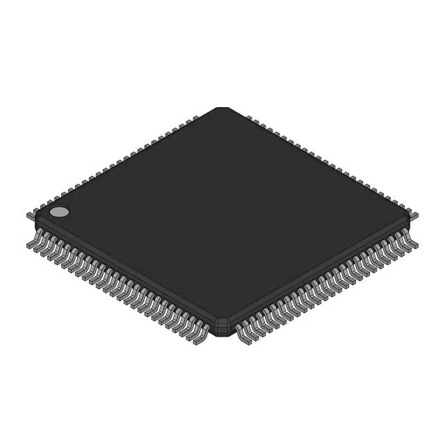
100-TQFP (14x14 mm) with 0.5 mm pitch — the same footprint as many mid-density synchronous SRAMs and NOR flash parts. The 100-LQFP case code means the body is 14 mm square with a 1.4 mm height; the exposed pad is absent on TQFP, so all thermal dissipation goes through the leads. A four-layer board with a solid ground plane under the package is the safe bet for signal integrity at 100 MHz. Bulk packaging — tray or tube, not tape-and-reel — so this is a prototyping or low-volume production buy. No reel fee, but the pick-and-place feeder needs a tray shaker or tube handler.
What the 8 ns access time means on the bench
8 ns access at 100 MHz is a 1-cycle latency on reads — the address is presented on clock edge N, data is valid on clock edge N+1. If the downstream FPGA or ASIC expects data on the same edge, the timing budget is tight: the 8 ns includes the clock-to-output delay plus the output hold time. A scope probe on the data lines with a 10 pF load will show the real edge rate; the datasheet's AC timing table is the reference, not the 100 MHz number alone.