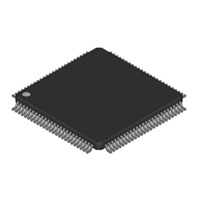
Renesas Electronics 71V3578S150PFG — DC-DC Power Modules

71V3578S150PFG 4.5Mbit Sync SRAM, 150 MHz, 3.8 ns Access

MPN71V3578S150PFG
End of Life

Renesas 71V3578S150PFG synchronous SRAM, 4.5 Mbit (256K x 18), 150 MHz clock frequency, 3.8 ns access time, parallel interface, 3.135-3.465 V supply, 0°C to 70°C, 100-TQFP (14x14 mm).

$4.11Ref. price · indicative, final on quote
Packaging100-LQFP
StockContact for availability
MOQ1 pcs
  • 100% new & originalTraceable channels only — no refurbs, no pulls, no remarked parts.
  • Date & lot codes on quoteStated per line before you commit; label photos on request.
  • MSL-compliant ESD packingMoisture-sealed bags with indicator cards; reels photo-verified.
  • PayPal buyer protectionPay by T/T, PayPal or Payoneer — card payments covered end to end.

Specifications

71V3578S150PFG Technical Specifications
ParameterValue
Memory typeVolatile
Mounting typeSurface Mount
Voltage3.135V ~ 3.465V
Frequency150 MHz
Memory interfaceParallel
Operating temperature0°C ~ 70°C (TA)
PackageBulk
TechnologySRAM - Synchronous, SDR
Access time3.8 ns
Memory size4.5Mbit
Memory formatSRAM
Case100-LQFP
Memory organization256K x 18

Product details

Synchronous SRAM at 150 MHz — what the ratings mean for the bus

The Renesas 71V3578S150PFG is a 4.5 Mbit synchronous SRAM organized as 256K x 18 bits, clocked at 150 MHz with a 3.8 ns access time.

Supply and temperature — the operating envelope

Supply range is 3.135 V to 3.465 V. Operating temperature is 0°C to 70°C.

Package and mounting

Housed in a 100-LQFP (supplier device package 100-TQFP, 14x14 mm body).

Lifecycle and sourcing

The 71V3578S150PFG carries an active lifecycle status — no last-time-buy notice, no end-of-life risk on the immediate horizon. It remains a current-production part, which simplifies BOM planning for new designs and avoids the premium pricing that obsolete synchronous SRAMs often command on the surplus market. For a BOM freeze or a production ramp, this part can be qualified into the supply chain without the clock ticking on availability.

Frequently asked questions

What is the access time of 71V3578S150PFG?

The access time is 3.8 ns. At a 150 MHz clock (6.67 ns period), this leaves roughly 2.9 ns of timing margin for the receiving logic after the data becomes valid — a figure that needs careful PCB trace-length matching and signal-integrity analysis to close timing.

What voltage does the 71V3578S150PFG use?

The supply voltage range is 3.135 V to 3.465 V — a standard 3.3 V rail with ±5 % tolerance. The system's 3.3 V supply must stay within this window at the device pins, accounting for IR drop across the PCB.

What is the memory organization of 71V3578S150PFG?

Organized as 256K words by 18 bits, for a total of 4.5 Mbit. The x18 width is useful for 16-bit data with two parity bits, or for DSP systems that process 18-bit fixed-point words natively.