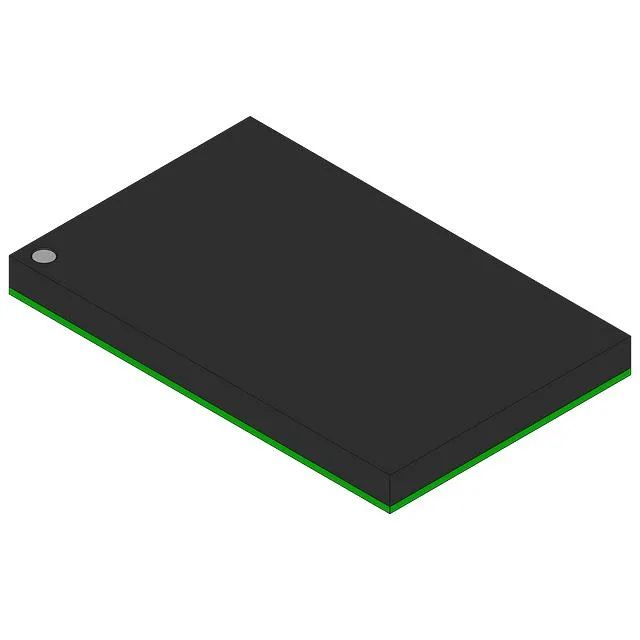
The 71V3577S85BGI comes in a 119-ball BGA (14x22 mm body) — the same footprint used across Renesas' synchronous SRAM family. The 1.0 mm ball pitch demands a multi-layer PCB with microvias or blind vias for fan-out; a two-layer board will not break out the inner rows. It is supplied in Bulk — tray or tube, not tape-and-reel — which is typical for prototype or repair quantities. For volume pick-and-place, confirm the carrier format with your assembler.
Timing and bus interface
This is a synchronous SDR (Single Data Rate) SRAM — the address and control are latched on the rising edge of the clock, and data is driven out on the next clock edge. The 8.5 ns access time is the delay from clock edge to valid data; at 87 MHz (11.5 ns period), the access window is tight but within spec for a 3-3-3-3 burst. The 128K x 36 organization gives a 36-bit word width — common for processor local memory, cache tag stores, or network packet buffers where a wide data path reduces the number of chips. The parallel interface is straightforward: address, data, chip enable, output enable, and byte write enables.
The core and I/O share this supply, so the decoupling strategy is simpler than a dual-voltage SRAM. The 119-PBGA package's thermal resistance is not listed, but the 14x22 mm body with a solid ground plane underneath keeps the junction within limits at the rated clock.