What this synchronous SRAM brings to the bus
The Renesas 71V3558S133PFGI is a 4.5 Mbit synchronous SRAM organized 256K x 18, built on a ZBT architecture. It clocks at 133 MHz with a 4.2 ns access time.
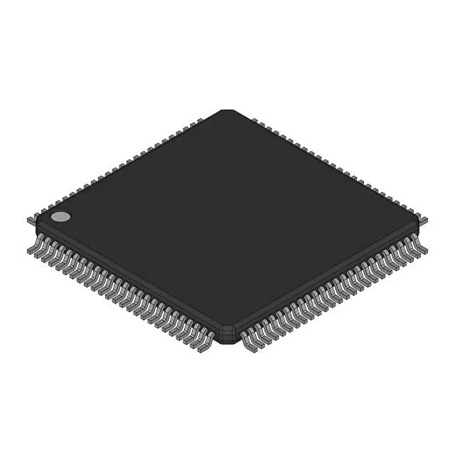
Renesas 71V3558S133PFGI, 4.5Mbit Synchronous SRAM (ZBT), 256K x 18, 133 MHz clock, 4.2 ns access, Parallel interface, 3.135V-3.465V supply, -40 to 85°C, 100-TQFP (14x14), Active.
| Parameter | Value |
|---|---|
| Memory type | Volatile |
| Mounting | Surface Mount |
| Supply voltage | 3.135V ~ 3.465V |
| Clock frequency | 133 MHz |
| Memory interface | Parallel |
| Operating temperature | -40°C ~ 85°C (TA) |
| Package | Bulk |
| Technology | SRAM - Synchronous, SDR (ZBT) |
| Access time | 4.2 ns |
| Memory size | 4.5Mbit |
| Memory format | SRAM |
| Case | 100-LQFP |
| Memory organization | 256K x 18 |
The Renesas 71V3558S133PFGI is a 4.5 Mbit synchronous SRAM organized 256K x 18, built on a ZBT architecture. It clocks at 133 MHz with a 4.2 ns access time.
The access time is 4.2 ns. Combined with the 133 MHz clock rate, this gives about 3.3 ns of timing margin for setup and hold in a typical synchronous memory controller design.
It comes in a 100-lead LQFP (also specified as 100-TQFP) with a 14x14 mm body — a fine-pitch surface-mount package that requires careful PCB layout for 133 MHz signal integrity.
It is organized as 256K words by 18 bits (4.5 Mbit total). The 18-bit width is typical for designs that need a parity or ECC bit per 16-bit word, or for 9-bit byte-oriented datapaths.