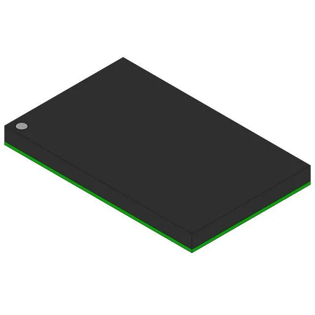
Renesas Electronics 71V2556SA133BGI — Discrete Semiconductors

Renesas 71V2556SA133BGI SRAM, 4.5Mbit, 133 MHz, 4.2 ns

MPN71V2556SA133BGI
End of Life

Renesas Electronics 71V2556SA133BGI, Synchronous SRAM (ZBT), 4.5Mbit, 133 MHz, 4.2 ns, Parallel, 3.135V-3.465V, -40°C to +85°C, 119-PBGA.

$5.8Ref. price · indicative, final on quote
Packaging119-BGA
Independent supplier — new & surplus stockAuthenticity-screened · ESD-safe packingListing updated Aug 2026

Specifications

71V2556SA133BGI specifications
ParameterValue
Memory typeVolatile
MountingSurface Mount
Supply voltage3.135V ~ 3.465V
Clock frequency133 MHz
Memory interfaceParallel
Operating temperature-40°C ~ 85°C (TA)
PackageBulk
TechnologySRAM - Synchronous, SDR (ZBT)
Access time4.2 ns
Memory size4.5Mbit
Memory formatSRAM
Case119-BGA
Memory organization128K x 36

Product details

Synchronous SRAM for high-throughput data buffering

The Renesas 71V2556SA133BGI is a 4.5 Mbit synchronous SRAM organized as 128K x 36 bits, using a Zero Bus Turnaround (ZBT) architecture that eliminates dead cycles between read and write operations on the same data bus. Rated for a 133 MHz clock and a 4.2 ns access time, this part is suited for high-throughput data buffering in networking, telecom, and test equipment where the bus must switch direction every cycle without a wait state.

119-PBGA footprint and layout considerations

Housed in a 119-ball PBGA (14x22 mm body), the part requires a multi-layer PCB for fan-out of the fine-pitch BGA balls — the 0.80 mm or 1.00 mm ball pitch typical of this package family does not route out on two layers.

Frequently asked questions

What is the memory organization of the 71V2556SA133BGI?

The 4.5 Mbit SRAM is organized as 128K words by 36 bits, providing a 36-bit-wide data bus for parity or ECC applications without external byte-masking logic.

What package does the 71V2556SA133BGI use?

It comes in a 119-ball PBGA (Plastic Ball Grid Array) with a 14x22 mm body, surface-mount for reflow soldering.