Speed-grade fit for the memory controller
The 71V016SA20YI is a 1 Mbit asynchronous SRAM from Renesas, organized 64K x 16 with a 20 ns access time. That 20 ns figure sets the ceiling for how fast the memory controller can read or write a word — the controller's setup and hold times plus the bus propagation delay must sum to less than 20 ns for a zero-wait-state cycle. This part sits in the speed bin that covers most 16-bit microcontroller and DSP designs running at 25-40 MHz bus clocks. The parallel interface means each address and data line is a dedicated pin — 20 address lines for the 64K word space plus 16 data lines. The PCB trace routing must match lengths within the 20 ns window, especially on the data bus, to avoid skew that eats into the access time budget.
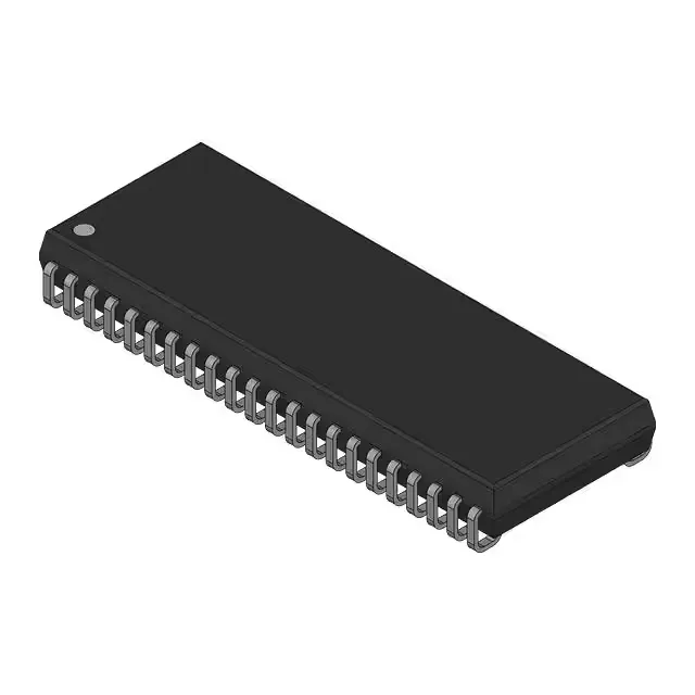
The 300 mV tolerance means the rail must stay within regulation — a 3.3 V supply with ±5% tolerance keeps the part inside its window, but a rail that dips to 3.0 V at full load still meets the minimum. The 44-SOJ package is a surface-mount J-bend footprint with a 0.400-inch body width. The J-lead form factor gives a smaller footprint than a DIP but still allows visual inspection of the solder joints.
Write timing and bus compatibility
This symmetry simplifies the memory controller timing — the same bus cycle works for both read and write without separate timing modes. The write pulse width must be held for the full 20 ns; a controller that stretches the write strobe to 25 ns still meets the spec, but one that pulses shorter than 20 ns risks data corruption on the trailing edge. As an asynchronous SRAM, this part needs no clock — the address lines are latched on the falling edge of the chip enable or write enable, whichever comes last. This makes it a drop-in replacement for legacy 64K x 16 SRAM sockets in designs that cannot tolerate the added latency of a synchronous burst interface.
Compliance and lifecycle posture
For a BOM that already carries this part number, the active status means no last-time-buy planning is needed.