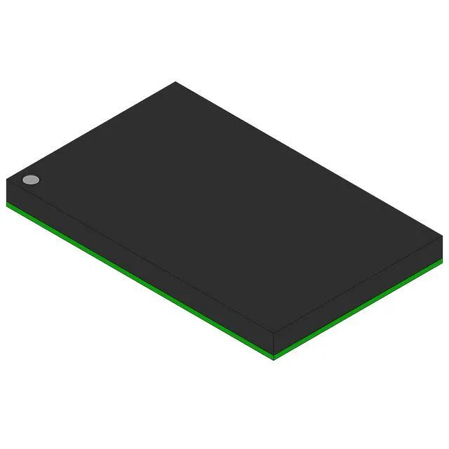
119-ball BGA footprint and reflow profile
The 71T75802S100BG: The 119-ball array requires a 4-layer PCB minimum for fan-out; the inner rows route through via-in-pad or microvia layers. The package has no exposed thermal pad — junction-to-board thermal resistance is set by the BGA ball count and the copper plane area under the device. A 1% or better regulator is recommended to stay within the tolerance band, especially when the SRAM shares the rail with other 2.5 V logic. Decouple with a 0.1 µF ceramic per supply pin and a 10 µF bulk cap within 10 mm of the package.
Synchronous ZBT SRAM — timing and throughput
This is an 18 Mbit synchronous SRAM using Zero Bus Turnaround (ZBT) technology, organized as 1M x 18 bits. The parallel interface runs at 100 MHz with a 5 ns access time from clock edge. ZBT eliminates the dead bus cycle between read and write operations, sustaining full throughput on a shared data bus — a common requirement in network buffers, test equipment, and DSP memory banks. The 5 ns access time at 100 MHz clock means the output data is valid 5 ns after the clock edge, giving the controller a 5 ns setup window before the next clock. This timing budget demands a matched-length PCB trace layout between the SRAM and the controller to avoid hold-time violations.