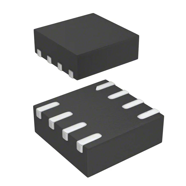
Renesas Electronics 621SCMGI8 — Clock & Timing ICs

Renesas 621SCMGI8 Clock Buffer, 1:4, 200 MHz, 8-VFQFN

MPN621SCMGI8
End of Life

Renesas 621SCMGI8 Clock Buffer, 1:4 fanout, 200 MHz max frequency, 1.71V–3.465V supply, -40°C to 105°C, 8-VFQFN (2x2) package, single-ended input/output.

$3.21Ref. price · indicative, final on quote
Packaging8-UFDFN
StockContact for availability
MOQ1 pcs
  • 100% new & originalTraceable channels only — no refurbs, no pulls, no remarked parts.
  • Date & lot codes on quoteStated per line before you commit; label photos on request.
  • MSL-compliant ESD packingMoisture-sealed bags with indicator cards; reels photo-verified.
  • PayPal buyer protectionPay by T/T, PayPal or Payoneer — card payments covered end to end.

Specifications

621SCMGI8 Technical Specifications
ParameterValue
TypeClock Buffer
Mounting typeSurface Mount
Voltage1.71V ~ 3.465V
Frequency200 MHz
Operating temperature-40°C ~ 105°C (TA)
InputClock
OutputClock
PackageTape & Reel (TR); Cut Tape (CT)
Case8-UFDFN
Number of circuits1
Ratio - Input:Output1:4
Differential - Input:OutputNo/No

Product details

What this 1:4 clock buffer is and where it fits

The Renesas 621SCMGI8 is a single-ended clock buffer that takes one clock input and drives four copies at up to 200 MHz. It is designed for general-purpose clock distribution on boards that need to fan out a reference clock to multiple loads.

200 MHz ceiling and single-ended I/O — what they mean for the design

The 200 MHz maximum frequency covers most SPI, I2S, and parallel-bus clock trees, but it is not a differential buffer (No/No on both input and output). That means it cannot cleanly propagate a high-speed differential clock like LVPECL or LVDS — for those, look at a dedicated fanout buffer such as the 8SLVP2108. The single-ended input also means the device is sensitive to noise on the clock trace; keep the trace short and run a solid ground plane underneath. The 1:4 ratio is fixed — no configurability — so if you need a 1:2 or 1:8 fanout, this part does not stretch.

Supply and temperature — industrial range, wide voltage

The 1.71 V to 3.465 V supply covers the three common digital rail voltages: 1.8 V, 2.5 V, and 3.3 V. At 1.8 V the margin is tight — the minimum is 1.71 V, so a 1.8 V rail with a 5% tolerance (1.71 V) just meets the spec. If your rail sags under load, consider a 2.5 V or 3.3 V supply for headroom. The -40°C to 105°C range is full industrial; the part can sit in an unventilated enclosure or near a warm processor without derating.

Package and footprint — 8-VFQFN (2x2 mm)

The 621SCMGI8 comes in an 8-VFQFN package with a 2 mm x 2 mm body (supplier device package 8-VFQFN). It is a surface-mount, leadless package with an exposed pad — the pad should be soldered to a ground plane for thermal and electrical continuity.

Lifecycle and sourcing reality

The 621SCMGI8 is listed as Active on the manufacturer's status — no last-time-buy or end-of-life notice. It is RoHS3 compliant. For a BOM line, this means no imminent obsolescence risk and no need to qualify a substitute for production. The closest functional peer is the 5PB1104CMGK/W from the same family: same 1:4 ratio, same 200 MHz ceiling, same LVCMOS output type, same supply and temperature range. The difference is the package — the 5PB1104 comes in a different 8-pin package — so verify footprint compatibility before swapping.

Frequently asked questions

Is 621SCMGI8 compatible with 1.8V input logic?

Yes, the supply range includes 1.71 V to 3.465 V, so a 1.8 V input clock is within spec as long as the supply is at least 1.71 V.

What is the equivalent or cross reference for 621SCMGI8?

The closest functional equivalent is the 5PB1104CMGK/W, which has the same 1:4 fanout, 200 MHz max, LVCMOS output, and industrial temp range. The packages differ — verify footprint compatibility before substituting.