PLL with bypass — glitch-free clock switching for redundant timing
The 5V49EE501NLGI integrates a PLL with bypass mode, meaning the output can switch between a synthesized clock and a clean reference without the PLL re-lock transient. This is the architecture you want when a redundant oscillator or holdover source must take over without corrupting the downstream SERDES or FPGA transceiver link. The PLL accepts LVCMOS, LVTTL, or crystal inputs and produces differential outputs (HCSL, LVDS, LVPECL) alongside single-ended LVCMOS/LVTTL — the differential-to-single-ended conversion is handled on-chip, so no external level translator is needed between the crystal and the high-speed output lines.
500 MHz ceiling — what it means for the clock tree
The maximum output frequency of 500 MHz covers PCIe Gen1/2/3 reference clocks (100 MHz), 10GbE (156.25 MHz), and most FPGA transceiver reference frequencies up to the mid-hundreds of megahertz. The divider/multiplier pair (Yes/Yes) lets you synthesize non-standard frequencies from a common crystal — a 25 MHz input multiplied to 125 MHz for Ethernet, for example. The 2:5 input-to-output ratio means two input sources (e.g., primary crystal and secondary LVCMOS) can be fanned out to five clock domains. This covers a typical SoC clock tree: one output for the core, one for the memory controller, one for the PCIe block, and two spare for peripheral interfaces.
Industrial temperature range and supply tolerance
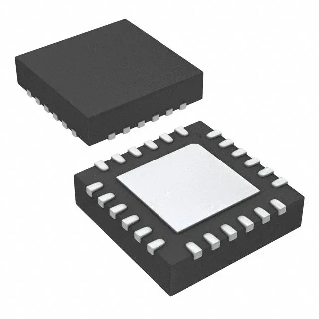
The 24-QFN (4x4 mm) package with exposed pad provides a low-inductance ground path for the high-speed differential outputs.
Active lifecycle — no LTB pressure on this BOM line
This part is safe to specify into a new design without planning a migration for the next three to five years. The VersaClock III family has broad installed base, so cross-reference data and application notes are readily available.