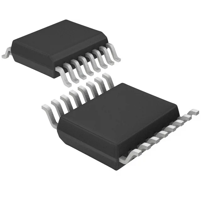
Renesas Electronics 5V41235PGG — Clock & Timing ICs

Renesas 5V41235PGG PCIe Clock Generator, 200MHz, 16-TSSOP

MPN5V41235PGG
End of Life

Renesas Electronics 5V41235PGG PCI Express (PCIe) clock generator IC, PLL Yes, 200 MHz max, HCSL/LVDS outputs, 1:2 fanout, 16-TSSOP package, Tube.

$3.83Ref. price · indicative, final on quote
Packaging16-TSSOP (0.173", 4.40mm Width)
StockContact for availability
Lead timeIn Stock wk
MOQ1 pcs
  • 100% new & originalTraceable channels only — no refurbs, no pulls, no remarked parts.
  • Date & lot codes on quoteStated per line before you commit; label photos on request.
  • MSL-compliant ESD packingMoisture-sealed bags with indicator cards; reels photo-verified.
  • PayPal buyer protectionPay by T/T, PayPal or Payoneer — card payments covered end to end.

Specifications

5V41235PGG Technical Specifications
ParameterValue
Mounting typeSurface Mount
Voltage3.135V ~ 3.465V
Frequency200MHz
Operating temperature0°C ~ 70°C
PLLYes
InputClock, Crystal
OutputHCSL, LVDS
PackageTube
Main purposePCI Express (PCIe)
Case16-TSSOP (0.173\", 4.40mm Width)
Number of circuits1
Ratio - Input:Output1:2
Differential - Input:OutputNo/Yes

Product details

1:2 fanout PCIe clock generator in 16-TSSOP

The Renesas 5V41235PGG is a single-circuit PLL clock generator built for PCI Express (PCIe) reference-clock duty. It accepts a clock or crystal input and delivers two output banks in HCSL or LVDS signaling — the two dominant formats for PCIe clock distribution — at frequencies up to 200 MHz. The 1:2 input-to-output ratio means one reference source fans out to two independent clock lanes, covering the typical topology for a single PCIe root complex driving two endpoints.

200 MHz ceiling and supply tolerance

The 200 MHz maximum output frequency covers PCIe Gen1 (100 MHz), Gen2 (100 MHz), and Gen3 (100 MHz) reference clock requirements with margin. The differential outputs (No/Yes) mean the input side accepts a single-ended clock or crystal, while the output side drives differential HCSL or LVDS pairs — a common interface bridge for PCIe clock trees. Supply voltage spans 3.135 V to 3.465 V, a ±5 % window around the 3.3 V nominal rail. The commercial temperature grade (0 °C to 70 °C) limits deployment to indoor, temperature-controlled environments — not suitable for extended industrial or automotive ambient ranges.

Frequently asked questions

What is the closest functional alternative to 5V41235PGG?

The 5V41065PGG shares the same 1:2 fanout, 200 MHz maximum frequency, HCSL/LVDS outputs, and 16-TSSOP package. The 5V41066PGG offers a 1:4 fanout instead of 1:2, which matters if the board needs more clock lanes from a single PLL.

What PCIe generations does the 200 MHz maximum support?

200 MHz covers PCIe Gen1, Gen2, and Gen3 reference clock rates (100 MHz base) with headroom. It does not support the 400 MHz reference clock used in some Gen4/Gen5 implementations.