PCIe clock source with integrated PLL
The Renesas 5V41234NLGI is a single-circuit PLL-based clock generator purpose-built for PCI Express (PCIe) reference clocking. It accepts a single-ended LVCMOS or crystal input and produces a differential HCSL or LVDS output at up to 100 MHz, with a 1:1 input-to-output ratio. The part operates from a 3.135 V to 3.465 V supply and is rated over the industrial temperature range of -40°C to 85°C, making it suitable for outdoor telecom cabinets and factory-floor controllers that see thermal cycling.
Differential output, single-ended input — plan the input conditioning
The input side is not differential — it accepts LVCMOS or a crystal — so the board designer needs to provide a clean single-ended reference or a fundamental-mode crystal. The output side is differential (HCSL or LVDS), which is what the PCIe reference clock receiver expects. The 1:1 ratio means one input drives one output; no fanout inside this package.
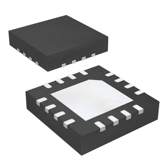
Housed in a 16-lead VFQFN with exposed pad (3 mm × 3 mm body), surface-mount only. Standard QFN reflow profile applies; MSL level is not in this record, so verify the moisture sensitivity label on the reel before opening the bag.