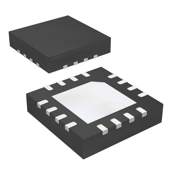
16-VFQFN 3x3 mm — PCIe reference clock with differential outputs
The 5V41064NLGI is a single-circuit PLL clock generator from Renesas, purpose-built for PCI Express (PCIe) reference clock generation. It accepts a clock or crystal input and delivers a 1:1 fanout to differential HCSL or LVDS outputs, with a maximum output frequency of 100 MHz. Housed in a 16-VFQFN exposed-pad package (3x3 mm body, supplier device package 16-VFQFPN), it is a surface-mount component. The exposed pad requires a thermal land pattern on the PCB for adequate heat transfer — the datasheet's recommended footprint should be followed for the pad and via array.
This makes it suitable for base-station, networking, and industrial computing environments where the ambient temperature inside the enclosure can exceed 70°C. The differential input-to-output relationship is No/Yes — the input is single-ended (clock or crystal), while the output is differential (HCSL or LVDS). This is the typical architecture for a PCIe reference clock buffer: a single-ended source fans out to a differential trace pair driving the PCIe root complex or switch.
Active production — sourcing and compliance
Renesas lists the 5V41064NLGI as Active product status, with ROHS3 compliance. The part is supplied in tube packaging. For BOM placement, the 5V41064NLGI is the industrial-temperature (-40°C to 85°C) tube-pack variant.